APPENDIX
Appendix 2. Control registers
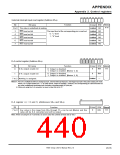
b7 b6 b5 b4 b3 b2 b1 b0
External interrupt input read register (Address 9516
)
Reference
Bit
Bit name
Function
At reset R/W
Undefined RO
Undefined RO
Undefined RO
Undefined RO
Undefined RO
Undefined RO
6-18
2 to 0 The value is undefined at reading.
3
4
5
6
7
INT3 read out bit
INT4 read out bit
INT5 read out bit
INT6 read out bit
INT7 read out bit
The input level at the corresponding pin is read out.
0 : “L” level
1 : “H” level
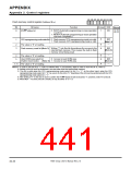
b7 b6 b5 b4 b3 b2 b1 b0
D-A control register (Address 9616)
Reference
Bit
0
Bit name
Function
0: Output is disabled.
At reset R/W
13-3
0
RW
RW
—
D-A
D-A
0
1
output enable bit
1: Output is enabled. (Notes 1, 2)
0: Output is disabled.
1: Output is enabled. (Notes 1, 2)
0
1
output enable bit
Undefined
7 to 2 Nothing is assigned.
Notes 1: Pin DAi is multiplexed with an analog input pin, external interrupt input pin, and trigger input pin in the pulse output port mode.
When a D-Ai output enable bit = “1” (in other words, output is enabled.), however, the corresponding pin cannot function as
any other multiplexed input/output pin (including a programmable I/O port pin).
2: When not using the D-A converter, be sure to clear this bit to “0.”
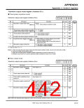
b7
b0
D-A register i (i = 0 and 1) (Addresses 9816 and 9916)
Bit
At reset
0
Reference
Function
R/W
RW
13-3
7 to 0 Any value in the range from 0016 through FF16 can be set (Note), and this
value will be D-A converted and will be output.
Note: When not using the D-A converter, be sure to clear the contents of these bits to “0016.”
7906 Group User’s Manual Rev.2.0
20-35

 RENESAS [ RENESAS TECHNOLOGY CORP ]