APPENDIX
Appendix 2. Control registers
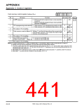
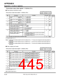
Three-phase output data register 1 (Address A916
)
ꢀ Three-phase waveform mode
b7 b6 b5 b4 b3 b2 b1 b0
Three-phase output data register 1 (Address A916
)
X
X
X
Function
Bit
0
Bit name
At reset R/W
Reference
W-phase fixed output’s polarity
10-11
0 : “H” output fixed
1 : “L” output fixed
0
0
0
RW
RW
RW
set bit
(Note 1)
0 : “H” output fixed
1 : “L” output fixed
V-phase fixed output’s polarity
set bit (Note 2)
1
2
0 : “H” output fixed
1 : “L” output fixed
U-phase fixed output’s polarity
set bit (Note 3)
Invalid in the three-phase waveform mode.
3
4
0
0
RW
RW
0 : “H” output
V-phase output polarity set buffer
(in three-phase mode 0)
1 : “L” output
0 : Every second time
1 : Every forth time
Interrupt request interval set bit
(in three-phase mode 1)
0 : “H” output
1 : “L” output
U-phase output polarity set buffer
(in three-phase mode 0)
5
0
0
RW
RW
0 : An interrupt request occurs at each even-number-
ed underflow of timer A3
1 : An interrupt request occurs at each odd-number-
ed underflow of timer A3
Interrupt validity output select bit
(in three-phase mode 1)
7, 6
Invalid in the three-phase waveform mode.
X: It may be either “0” or “1.”
Notes 1: Valid when the W-phase output fix bit (bit 0 at address A816) = “1.” Be sure not to change the value during output of a
fixed value.
2: Valid when the V-phase output fix bit (bit 1 at address A816) = “1.” Be sure not to change the value during output of a
fixed value.
3: Valid when the U-phase output fix bit (bit 2 at address A816) = “1.” Be sure not to change the value during output of a
fixed value.
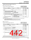
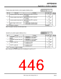
ꢀ Pulse output port mode
b7 b6 b5 b4 b3 b2 b1 b0
Three-phase output data register 1 (Address A916
)
X X
Function
Bit
0
Bit name
At reset R/W
Reference
Pulse width modulation enable
bit 0
0 : No pulse width modulation by timer A1
1 : Pulse width modulation by timer A1
9-7
0
0
0
0
0
RW
RW
RW
RW
RW
0 : No pulse width modulation by timer A2
1 : Pulse width modulation by timer A2
Pulse width modulation enable
bit 1
1
2
0 : No pulse width modulation by timer A4
1 : Pulse width modulation by timer A4
Pulse width modulation enable
bit 2
Pulse output polarity select bit
0 : Positive
1 : Negative
3
4
RTP1
0
pulse output data bit
(Valid in pulse mode 0) (Note)
0 : “L” level output
1 : “H” level output
5
RTP1
1
pulse output data bit
0
RW
(Valid in pulse mode 0) (Note)
Invalid in pulse output port mode.
6
7
0
0
RW
RW
X: It may be either “0” or “1.”
Note: Invalid in pulse mode 1.
7906 Group User’s Manual Rev.2.0
20-40

 RENESAS [ RENESAS TECHNOLOGY CORP ]