PULSE OUTPUT PORT MODE
9.4 Setting of pulse output port mode
Continued from preceding Figure 9.4.1.
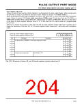
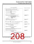
Registers used in pulse output port 1
Pulse output data register 0
Processing of avoiding undefined output before starting pulse output (Note)
b7
0
b0
Three-phase output data register 0 (Address A816
)
0
(Address A216
)
0
RTP0
RTP0
RTP0
RTP0
RTP1
RTP1
1
2
3
Initial output data is set.
0
1
Pulse output trigger select bits
Underflow of Timer A0
b7
b0
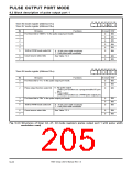
Pulse output data register 1
(Address A416
Three-phase output data register 1 (Address A916
)
✽
✽
✽ ✽
)
Pulse width modulation enable bit 0
Pulse width modulation enable bit 1
Pulse width modulation enable bit 2
See Table 9.2.3.
Pulse output polarity select bit
0 : Positive
1 : Negative
X : It may be either “0” or “1.”
b7
b0
0
Timer A0 mode register (Address 5616
)
Timer A5 mode register
(Address D16
0
0
0
0
0
0
0
)
Selection of count source f
2
(b15)
b7
(b8)
b0 b7
b0
Timer A0 register (Addresses 4716 and 4616
)
Timer A5 register
(Addresses C716, C616
0016
0016
)
A value of “000016” is set.
b7
b7
b0
Timer A0 interrupt control register (Address 7516
)
Timer A5 interrupt control register
(Address F516
0
0
0
0
)
Interrupt disabled
No interrupt request
b0
Count start register 0 (Address 4016
)
Count start register 1
(Address 4116
)
Timer A0 count start bit
1 : Start counting
When an underflow occurs in timer A0, the contents of three-phase output data register 0 are output from the filp-flop.
(Pulse output pins are floating until the pulse output becomes enabled.)
b7
b0
Count start register 1
(Address 4116
Count start register 0 (Address 4016
)
)
Timer A0 count start bit
0 : Stop counting
This processing can be omitted when the system is not
affected by the undefined output.
Continued on Figure 9.4.3.
Fig. 9.4.2 Initial setting example for registers relevant to pulse output port 0 (pulse mode 1) (2)
7905 Group User’s Manual Rev.1.0
9-27

 RENESAS [ RENESAS TECHNOLOGY CORP ]