PULSE OUTPUT PORT MODE
9.2 Block description of pulse output port 0
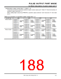
9.2.3 Port P5 direction register
The pulse output trigger input pin is multiplexed with port P5
When using pin P5 /RTPTRG0 as a pulse output trigger input pin, be sure to clear the port P5 direction
register’s bit, corresponding to port P5 pin, in order to set this port P5 pin for the input mode.
3
pin.
3
3
3
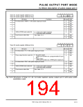
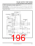
Figure 9.2.4 shows the relationship between port P5 direction register and a pulse output trigger input pin.
b7 b6 b5 b4 b3 b2 b1 b0
Port P5 direcition register (Address D16
)
Bit
0
Corresponding pin
Nothing is assigned.
Function
At reset R/W
—
Undefined
0 : Input mode
1 : Output mode
Pin INT1
RW
RW
RW
—
1
0
0
0
Pin INT2/RTPTRG1
Pin RTPTRG0 (Pin INT3)
Nothing is assigned.
Pin INT5/TB0IN/IDW
2
When using this pin as a pulse output trigger
input pin, be sure to clear the corresponding bit to “0.”
3
4
Undefined
0 : Input mode
1 : Output mode
5
RW
RW
RW
0
0
0
6
Pin INT6/TB1IN/IDV
Pin INT7/TB2IN/IDU
7
Note: ( ) shows the I/O pin of another internal peripheral device which is multiplexed.
Fig. 9.2.4 Relationship between port P5 direction register and pulse output trigger input pin
7905 Group User’s Manual Rev.1.0
9-11

 RENESAS [ RENESAS TECHNOLOGY CORP ]