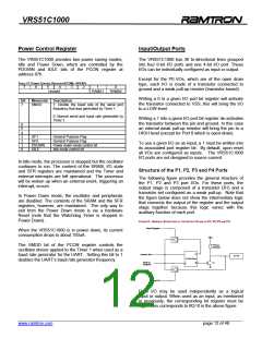
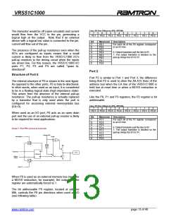
VRS51C1000
When the port is used as an output, the register
contains information on the state of the output pins.
Measuring the state of an output directly on the pin is
inaccurate because the electrical level depends mostly
on the type of charge that is applied to it. The functions
shown below take the value of the register rather than
that of the pin.
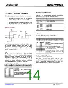
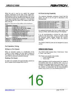
I/O Ports Driving Capability
The maximum allowable continuous current that the
device can sink on an I/O port is described in the
following table.
Maximum sink current on one given I/O
Maximum total sink current for P0
Maximum total sink current for P1, 2, 3
Maximum total sink current for P4
Maximum total sink current on all I/O
10mA
26mA
15mA
20mA
91mA
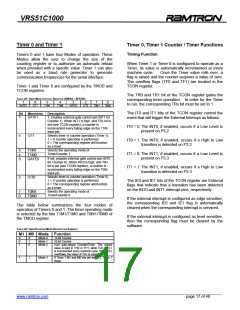
TABLE 24: LIST OF INSTRUCTIONS THAT READ AND MODIFY THE PORT USING REGISTER
VALUES
Instruction Function
ANL
ORL
XRL
JBC
CPL
INC
Logical AND ex: ANL P0, A
Logical OR ex: ORL P2, #01110000B
Exclusive OR ex: XRL P1, A
Jump if the bit of the port is set to 0
Complement one bit of the port
Increment the port register by 1
Decrement the port register by 1
Decrement by 1 and jump if the result is not
equal to 0
As explained previously, the Port 4 output buffers can
sink up to 20mA, which allow driving of LED displays.
It is not recommended to exceed the sink current
outlined in the above table. Doing so is likely to make
the low-level output voltage exceed the device’s
specification and it is likely to affect the device’s
reliability.
DEC
DJNZ
MOV P.,C
CLR P.x
Copy the held bit C to the port
Set the port bit to 0
SETB P.x
Set the port bit to 1
The VRS51C1000 I/O ports are not designed to source
current.
Port Operation Timing
Writing to a Port (Output)
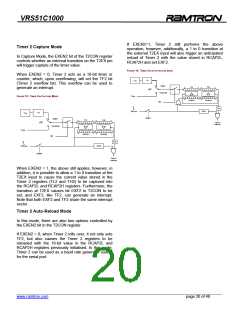
VRS51C1000 Timers
When an operation results in a modification of the
content in a port register, the new value is placed at
the output of the D flip-flop during the last machine
cycle that the instruction needed to execute.
The VRS51C1000 includes three 16-bit timers: Timer
0, Timer 1 and Timer 2.
The Timers can operate in two modes:
o
o
Event counting mode
Timer mode
Reading a Port (Input)
In order to be sampled, the signal duration present on
the I/O inputs must be longer than Fosc/12.
When operating in event counting mode, the counter is
incremented each time an external event, such as a
transition in the logical state of the Timer input (T0, T1,
T2 input), is detected. When operating in Timer mode,
the counter is incremented by the microcontroller’s
system clock (Fosc/12) or by a divided version of it.
______________________________________________________________________________________________
www.ramtron.com page 16 of 48

 RAMTRON [ RAMTRON INTERNATIONAL CORPORATION ]