VRS51C1000
TABLE 18: PORT 0 REGISTER (P0) - SFR 80H
The transistor would be off (open-circuited) and current
would flow from the VCC to the pin, generating a
logical high at the output. Note that if an external
device with a logical low value is connected to the pin,
current will flow out of the pin.
7
6
5
4
3
P0.3
2
P0.2
1
P0.1
0
P0.0
P0.7
P0.6
P0.5
P0.4
Bit
7
6
5
4
3
2
1
0
Mnemonic Description
P0.7
P0.6
P0.5
P0.4
P0.3
P0.2
P0.1
P0.0
For each bit of the P0 register correspond
to an I/O line:
The presence of the pull-up resistance even when the
I/O’s are configured as inputs means that a small
current is likely to flow from the VRS51C1000 I/O’s
pull-up resistors to the driving circuit when the inputs
are driven low. For this reason, the VRS51C1000 I/O
ports P1, P2, P3 and P4 are called “quasi bi-
directional”.
0: Output transistor pull the line to 0V
1: The output transistor is blocked so the
pull-up brings the I/O to 5V.
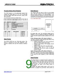
Port 2
Structure of Port 0
Port P2 is similar to Port 1 and Port 3, the difference
being that P2 is used to drive the A8-A15 lines of the
address bus when the EA line of the VRS51C1000 is
held low at reset time or when a MOVX instruction is
executed.
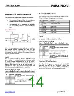
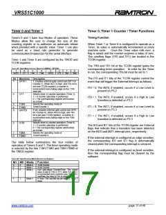
The internal structure of P0 is shown in the next figure.
As opposed to the other ports, P0 is truly bi-directional.
In other words, when used as an input, it is considered
to be in a floating logical state (high impedance state).
This arises from the absence of the internal pull-up
resistance. The pull-up resistance is actually replaced
by a transistor that is only used when the port is
configured for accessing external memory/data bus
(EA=0).
Like the P0, P1 and P3 registers, the P2 register is bit
addressable.
TABLE 19: PORT 2 REGISTER (P2) - SFR A0H
7
6
5
4
3
2
1
0
P2.7
P2.6
P2.5
P2.4
P2.3
P2.2
P2.1
P2.0
When used as an I/O port, P0 acts as an open drain
port and the use of an external pull-up resistor is likely
to be required for most applications.
Bit
7
6
5
4
3
2
1
0
Mnemonic Description
P2.7
P2.6
P2.5
P2.4
P2.3
P2.2
P2.1
P2.0
For each bit of the P2 register correspond
to an I/O line:
0: Output transistor pull the line to 0V
1: The output transistor is blocked so the
pull-up brings the I/O to 5V.
FIGURE 7: PORT P0’S PARTICULAR STRUCTURE
Address A0/A7
Read Register
Control
Vcc
Q
Internal Bus
IC Pin
D Flip-Flop
X1
Write to
Register
Q
Read Pin
When P0 is used as an external memory bus input (for
a MOVX instruction, for example), the outputs of the
register are automatically forced to 1.
The bit addressable P0 register, located at address
80h, controls the P0 pin directions when used as I/O
(see following table).
______________________________________________________________________________________________
www.ramtron.com page 13 of 48

 RAMTRON [ RAMTRON INTERNATIONAL CORPORATION ]