VRS51C1000
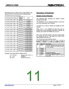
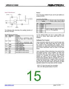
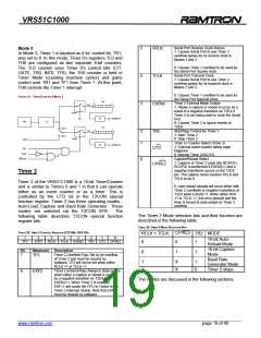
FIGURE 9: P3 PORT STRUCTURE
Port 4
Auxiliary
Function: Output
Read Register
Port 4 has four related I/O pins and its port address is
located at 0D8H.
Vcc
IC Pin
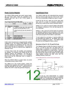
TABLE 23: PORT 4 (P4) - SFR D8H
X1
7
6
5
4
3
2
1
0
Q
Internal Bus
Unused
P4.3
P4.2
P4.1
P4.0
D Flip-Flop
Write to
Register
Q
Bit
Mnemonic Description
7
6
5
4
3
2
1
0
Unused
Unused
Unused
Unused
P4.3
P4.2
P4.1
P4.0
-
-
-
-
Read Pin
Auxiliary
Function: Input
Used to output the setting to pins P4.3,
P4.2, P4.1, P4.0 respectively.
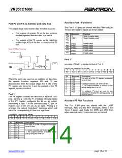
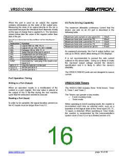
The following table describes the auxiliary function of
the Port 3 I/O pins.
TABLE 22: P3 AUXILIARY FUNCTION TABLE
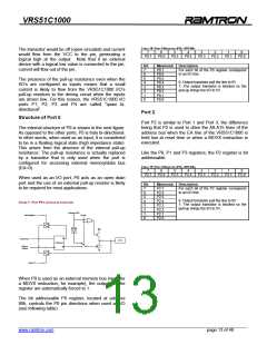
On the VRS51C1000, the Port 4 output buffers can
sink up to 20mA, which allow direct drive of LED
displays.
Pin
Mnemonic
Function
P3.0
RXD
Serial Port:
Receive data in asynchronous mode.
Input and output data in synchronous
mode.
Software Port Control
P3.1
TXD
Serial Port:
Transmit data in asynchronous mode.
Output clock value in synchronous mode.
External Interrupt 0
Timer 0 Control Input
External Interrupt 1
Some instructions allow the user to read the logic state
of the output pin, while others allow the user to read
the content of the associated port register. These
instructions are called read-modify-write instructions. A
list of these instructions may be found in the table
below.
P3.2
P3.3
INT0
INT1
Timer 1 Control Input
P3.4
P3.5
P3.6
T0
T1
Timer 0 Counter Input
Timer 1 Counter Input
Write signal for external memory
WR
RD
Upon execution of these instructions, the content of the
port register (at least 1 bit) is modified. The other read
instructions take the present state of the input into
account. For example, the instruction ANL P3,#01h
obtains the value in the P3 register; performs the
desired logic operation with the constant 01h; and re-
copies the result into the P3 register. When users want
to take the present state of the inputs into account,
they must first read these states and perform an AND
operation between the read value and the constant.
P3.7
Read signal for external memory
MOV A, P3; State of the inputs in the accumulator
ANL A, #01; AND operation between P3 and 01h
______________________________________________________________________________________________
www.ramtron.com page 15 of 48

 RAMTRON [ RAMTRON INTERNATIONAL CORPORATION ]