VRS51C1000
Auxiliary Port 1 Functions
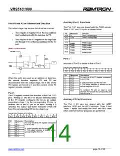
Port P0 and P2 as Address and Data Bus
The Port 1 I/O pins are shared with the PWM outputs,
Timer 2 EXT and T2 inputs as shown below:
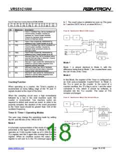
The output stage may receive data from two sources:
o
o
The outputs of register P0 or the bus address
itself multiplexed with the data bus for P0.
Pin
Mnemonic
Function
Timer 2 counter input
Timer2 Auxiliary input
P1.0 T2
P1.1 T2EX
P1.2
The outputs of the P2 register or the high byte
(A8 through A15) of the bus address for the P2
port.
P1.3
PWM0 output
PWM0
P1.4 PWM1
P1.5 PWM2
P1.6
PWM1 output
PWM2 output
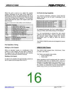
FIGURE 8: P2 PORT STRUCTURE
PWM3 output
PWM4 output
PWM3
Read Register
P1.7
PWM4
Vcc
Address
Pull-up
Network
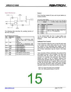
Port 3
Q
Q
Internal Bus
IC Pin
structure of Port 3 is similar to that of Port 1.
D Flip-Flop
Write to
Register
X1
Control
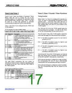
TABLE 21: PORT 3 REGISTER (P3) - SFR B0H
7
6
5
4
3
2
1
0
P3.7
P3.6
P3.5
P3.4
P3.3
P3.2
P3.1
P3.0
Read Pin
Bit
7
6
5
4
3
2
1
0
Mnemonic Description
P3.7
P3.6
P3.5
P3.4
P3.3
P3.2
P3.1
P3.0
For each bit of the P3 register correspond
to an I/O line:
When the ports are used as an address or data bus,
the special function registers P0 and P2 are
disconnected from the output stage, the 8 bits of the
P0 register are forced to 1 and the content of the P2
register remains constant.
0: Output transistor pull the line to 0V
1: The output transistor is blocked so the
pull-up brings the I/O to 5V.
To configure P3 pins as input or use
alternate P3 function the corresponding bit
must be set to 1.
Port 1
The P1 register controls the direction of the Port 1 I/O
pins. Writing a 1 into the P1.x bit (see following table)
of the P1 register configures the bit as an output,
presenting a logic 1 to the corresponding I/O pin, or
enables use of the I/O pin as an input. Writing a 0
activates the output “pull-down” transistor which will
force the corresponding I/O line to a logic Low.
Auxiliary P3 Port Functions
The Port 3 I/O pins are shared with the UART
interface, INT0 and the INT1 interrupts, Timer 0 and
Timer 1 inputs and finally the #WR and #RD lines
when external memory accesses are performed.
TABLE 20: PORT 1 REGISTER (P1) - SFR 90H
7
6
5
4
3
2
1
0
P1.7
P1.6
P1.5
P1.4
P1.3
P1.2
P1.1
P1.0
Bit
7
6
5
4
3
2
1
0
Mnemonic Description
P1.7
P1.6
P1.5
P1.4
P1.3
P1.2
P1.1
P1.0
For each bit of the P1 register correspond
to an I/O line:
0: Output transistor pull the line to 0V
1: The output transistor is blocked so the
pull-up bring the I/O to 5V.
______________________________________________________________________________________________
www.ramtron.com page 14 of 48

 RAMTRON [ RAMTRON INTERNATIONAL CORPORATION ]