©Quantum Research Group Ltd.
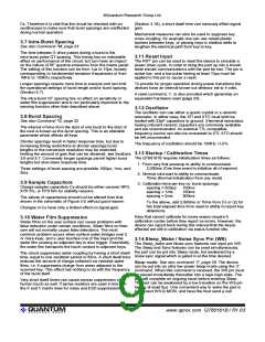
Table 1.1 Device Pin List
Pin
Name
Type Description
Master-Out / Slave In SPI line. In Master/Slave SPI mode is used for both communication directions.
1
MOSI
I/O PP
In Slave SPI mode is the data input (in only).
Master-In / Slave Out SPI line. Not used in Master/Slave SPI mode.
In Slave mode outputs data to host (out only).
SPI Clock. In Master mode is an output; in Slave mode is an input
Reset input, active low reset
+5V supply
2
MISO
I/O PP
3
SCK
RST
Vdd
I/O PP
I
Pwr
4
5
6
Vss
Pwr
O PP
I
Ground
7
XTO
XTI
Oscillator drive output. Connect to resonator or crystal.ply
Oscillator drive input. Connect to resonator or crystal, or external clock source.
UART receive input
8
9
RX
TX
I
10
11
12
13
14
15
16
17
18
19
20
21
22
23
24
25
26
27
28
29
30
31
32
33
34
35
36
37
38
39
40
41
42
43
44
O PP
I
UART transmit output
Wake from Sleep / Sync to noise source
Sample output control
WS
SMP
X0OPA
X1OPB
X2
O PP
I/O PP
I/O PP
O PP
O PP
Pwr
X0 Drive matrix scan / Communications option A input
X1 Drive matrix scan / Communications option B input
X2 Drive matrix scan
X3
Vdd
X3 Drive matrix scan
+5V supply
Vss
XS0
Pwr
I
Ground
XS0 Scan input line
XS1
XS2
I
XS1 Scan input line
XS2 Scan input line
I
XS3
I
XS3 Scan input line
YS0 Scan output line
YS0
YS1
YS2
YS3
AVdd
AGnd
Aref
O PP
O PP
O PP
O PP
Pwr
YS1 Scan output line
YS2 Scan output line
YS3 Scan output line
+5 supply for analog sections
Analog ground
Pwr
Pwr
+5 supply for analog sections
Cs3 control B
Cs3 control A
CS3B
CS3A
CS2B
CS2A
CS1B
CS1A
CS0B
CS0A
Vdd
I/O PP
I/O PP
I/O PP
I/O PP
I/O PP
I/O PP
I/O PP
I/O PP
Pwr
Cs2 control B
Cs2 control A
Cs1 control B
Cs1 control A
Cs0 control B
Cs0 control A
+5 supply
Ground
Vss
Pwr
LED
DRDY
Vref
O PP
O OD
I
Active low LED status drive / Activity indicator
Data ready output for Slave SPI mode; active low
Vref input for conversion reference
Oscilloscope sync output
SO
SS
O PP
I/O OD
Slave select for SPI direction control; active low
I/O: I = Input
O = Output
Pwr = Power pin
I/O = Bidirectional line
PP = Push Pull output drive
OD = Open drain output drive
lQ
iii
www.qprox.com QT60161B / R1.03

 QUANTUM [ QUANTUM RESEARCH GROUP ]