©Quantum Research Group Ltd.
Cx. Therefore it is vital that the circuit be checked with an (Section 3.18), a short dwell time can seriously affect signal
oscilloscope to make sure that burst spacings are unaffected gain.
during normal operation.
Mechanical measures can also be used to suppress key
cross-coupling, for example one can use raised plastic
barriers between keys, or placing keys in shallow wells to
lengthen the electrical path from key to key.
3.7 Intra-Burst Spacing
See also Command ^M, page 23
The time between X drive pulses during a burst is the
intra-burst pulse QT spacing. This timing has no noticeable
effect on performance of the circuit, but can have an impact
3.11 Reset Input
The RST’ pin can be used to reset the device to simulate a
on the nature of RF spectral emissions from the matrix panel. power down cycle, in order to bring the part up into a known
The setting of this function can be from 1µs to 10µs, loosely
corresponding to fundamental emission frequencies of from
1MHz to 100kHz respectively.
state should communications with the part be lost. The pin is
active low, and a low pulse lasting at least 10µs must be
applied to this pin to cause a reset.
Longer spacings require more time to execute and can limit
the operational settings of burst length and/or burst spacing
(Section 5.7).
To provide for proper operation during power transitions the
devices have an internal brown-out detector set to 4 volts.
A reset command, ‘r’, is also provided which generates an
equivalent hardware reset (page 25).
The intra-burst QT spacing has no effect on sensitivity or
water film suppression and is not particularly important to the
sensing function other than described above.
3.12 Oscillator
The oscillator can use either a quartz crystal or a ceramic
resonator. In either case, the XTI and XTO must both be
loaded with 22pF capacitors to ground. 3-terminal resonators
having onboard ceramic capacitors are commonly available
and are recommended. An external TTL-compatible
frequency source can also be connected to XTI; XTO should
be left unconnected.
3.8 Burst Spacing
See also Command ^G, page 22
The interval of time from the start of one burst to the start of
the next is known as the burst spacing. This is an alterable
parameter which affects all keys.
Shorter spacings result in faster response time, but due to
increasing timing restrictions at shorter spacings burst
lengths or the conversion resolution may be restricted,
limiting the amount of gain that can be obtained; see Sections
3.6 and 5.7. Conversely longer spacings permit higher burst
lengths but slow down response time.
The frequency of oscillation should be 12MHz +/-2%.
3.13 Startup / Calibration Times
The QT60161B requires initialization times as follows:
1. From very first powerup to ability to communicate:
2,000ms (One time event to initialize all of eeprom)
Three settings of burst spacing are possible: 500µs, 1ms, and
2ms.
2. Normal cold start to ability to communicate:
70ms (Normal initialization from any reset)
3.9 Sample Capacitors
Charge sampler capacitors Cs should be either ceramic NPO,
X7R 5%, or PPS film for stability reasons.
3. Calibration time per key vs. burst spacings:
spacing = 500µs: 100ms
spacing = 1ms:
spacing = 2ms:
150ms
300ms
The values of capacitance should not be altered from that
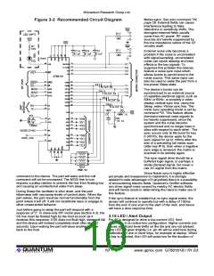
shown in the schematic of Figure 3-2 without good reason.
To the above, add 2,000ms or 70ms from (1) or (2) for
the total elapsed time from reset to ability to report key
detections.
Changes in Cs have only a limited effect on signal gain.
Keys that cannot calibrate for some reason require 5
calibration cycles before they report as errors. However, the
device can report back during this interval that the key(s)
affected are still in calibration via status function bits.
3.10 Water Film Suppression
Water films on the user surface can cause problems with
false detection under certain conditions. Water films on their
own will not normally cause false detections. The most
common problem occurs when surface water bridges over 2
or more keys, and a user touches one of the keys and the
water film causing an adjacent key to also trigger. Essentially,
the water film transports the touch contact to adjacent keys.
3.14 Sleep_Wake / Noise Sync Pin (WS)
The Sleep_wake and Noise sync features use input pin WS.
The Sleep and Sync features can be used simultaneously;
the part can be put into Sleep mode, but awakened by a
noise sync signal which is gated in at the time desired.
The circuit suppresses water coupling by having a short dwell
time, equal to one oscillator period or 83ns. A short dwell time
reduces the amount of charge collected via resistive water
films, i.e. it suppresses charge from areas adjacent to the
scanned key. This effect has nothing to do with the frequency
of the burst itself.
Sleep mode: See also command ‘Z’, page 25. The device
can be put into an ultra low-power sleep mode using the ‘Z’
command. When this command is received, the WS pin must
be placed immediately thereafter into a logic-high state. The
part will complete an ongoing burst before entering Sleep.
The part can be awakened by a low transition on the WS pin
lasting at least 5µs. One convenient way to wake the part is
to connect WS to MOSI, and have the host send a null
Very short dwell times can cause excess suppression of
human touch as well. If series resistors are used in line with
the X and Y matrix lines for noise and ESD suppression
lQ
9
www.qprox.com QT60161B / R1.03

 QUANTUM [ QUANTUM RESEARCH GROUP ]