©Quantum Research Group Ltd.
which limits the interval during which charge can be accepted interference in extreme cases. Such noise can be readily
suppressed by adding a 22pF capacitor from each Y line to
ground near the QT60161B.
by a Cs capacitor after the rise of an X drive line.
Dwell time has a dramatic effect on the suppression of
moisture films as described in Section 3.10.
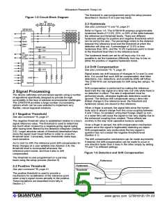
3.5 Burst Length & Sensitivity
See also Command ^F, page 21
Cs Charge Integrator capacitor. The Cs capacitors
integrate charge arriving through the matrix keys' Cx
capacitances, correspondent with the rise of X; to do this a
switching arrangement on the Cs control pins permits the
charge to accumulate so that the B side of the Cs capacitors
becomes negative when the A side is clamped to ground.
The signal gain in volts / pF of Cx for each key is controlled
by circuit parameters as well as the burst length.
The burst length is simply the number of times the
charge-transfer (‘QT’) process is performed on a given key.
Each QT process is simply the pulsing of an X line once, with
a corresponding Y line gated so as to capture the resulting
charge passed through the key’s capacitance Cx.
Charge conversion. At the end of each burst the voltage on
Cs is converted to digital by means of a single-slope
conversion process, using one of the external resistors to
ramp up the capacitor towards a reference voltage. The
elapsed time required to reach the comparison voltage is the
digital result. The time required to perform the conversion
depends on Cs, Cx, Rs, Aref, and the burst length.
QT60161B devices use a finite number of QT cycles which
are executed in a short burst. There can be from 1 to 64 QT
cycles in a burst, in accordance with the list of permissible
values shown on page 21. If a key's burst length is set to
zero, that burst is disabled but its time slot in the scanning
sequence of all keys is preserved so as to maintain scan
timing.
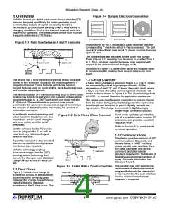
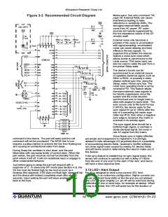
3.3 'X' Electrode Drives
The 'X' lines are directly connected to the matrix without
buffering. The positive edges of these signals are used to
create the transient field flows used to scan the keys. Only
one X line is actively driving the matrix for scanning purposes
at a time, and it will pulse repetitively for a ‘burst length’ for
each key as determined by the 'Burst Length' Setups
parameter (see command ^F, page 21 and Section 3.5).
Increasing burst length directly affects key sensitivity. This
occurs because the accumulation of charge on Cs is directly
linked to the burst length. The burst length of each key can be
set individually, allowing for direct digital control over the
signal gains of each key, indivudally.
3.3.1 RFI FROM X LINES
Apparent touch sensitivity is also controlled by the Negative
Threshold setting (Section 2.1). Burst length and negative
threshold interact; normally burst lengths should be kept as
short as possible to limit RF emissions, but the threshold
setting should normally be kept above a setting of 6 to limit
false detections. The detection integrator can also prevent
false detections at the expense of slower reaction times
(Section 2.6).
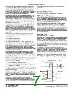
X drive lines will radiate a small amount of RFI. This can be
attenuated if required by using series resistor in-line with
each X trace; the resistor should be placed near to the
QT60161B. Typical values can range from 100 to 500 ohms.
Excessive amounts of R will cause a counterproductive drop
in signal strength. RC networks can also be used as shown in
Figure 4-6.
Resistance in the X lines also have the positive effect of
limiting ESD discharge currents (Section 3.18).
The value of Rs also affects sensitivity. Higher values of Rs
will lead to larger values of ADC result and higher conversion
gains. The side effect of this is that the conversion will take
longer and timing conflicts can occur (Section 3.6).
3.3.2 NOISE
C
OUPLING
I
NTO
X
LINES
External noise, sometimes caused by ground bounce due to
injected line noise, can couple into the X lines and cause
signal interference in extreme cases. Such noise can be
readily suppressed by the use of series resistors as
described above. Adding a small capacitor to the matrix line
on the QT60161B side of the R, for example 100pF to ground
near the QT60161B, will greatly help to reduce such effects.
Cs does not significantly affect gain. Smaller values of Cs will
have higher delta signal voltages but this gain increase is
offset by the decrease in gain caused by a steeper ADC
conversion slope. However smaller values of Cs lead to faster
conversion times for a given value of Rs, which in turn allows
for more relaxed burst timings. Smaller values of Cs also
reduce the dynamic range of the system, meaning that the
acquisition becomes less tolerant of high values of Cx, due to
earlier saturation of the voltage across Cs.
3.4 'Y' Gate Drives
There are 4 'Y' gate drive pairs (CS0A,B..CS3A,B); only one
pair of these lines is used during a burst for a particular key.
The magnitude of the voltages accumulated on the Cs
capacitors should never exceed 0.25V.
3.6 Burst Acquisition Duration
The total time required to acquire a key's signal depends on
the burst length for that key plus the time required to convert
the voltage on the corresponding Cs capacitor to digital. The
conversion is performed via a single-slope ADC process
using one of the external Rs resistors.
3.4.1 RFI FROM Y LINES
Y lines are nearly 'virtual grounds' and are negligible radiators
of RFI; in fact, they act as ‘sinks’ for RFI emitted by the X
lines. Resistors are not required in the Y lines for RFI
suppression, and in fact can introduce cross-talk among keys
if large enough. However, small resistance values can be
beneficial to limit ESD transients and make the circuit more
resistant to external RF fields (Section 3.18).
If the total time required for the acquisition, i.e. the burst
length plus ADC times plus the signal processing and serial
interface command handler times exceed the burst spacing
setup parameter (Section 3.8), significant timing errors and
communications problems can occur.
3.4.2 NOISE
C
OUPLING
INTO Y LINES
The time taken by the burst itself is straightforward to
quantify, but the time required to do the ADC step is not. The
ADC step depends on the value of Vref (pin 42), Cs, Rs, and
External noise, sometimes caused by ground bounce due to
power line noise, can couple into the Y lines and cause signal
lQ
8
www.qprox.com QT60161B / R1.03

 QUANTUM [ QUANTUM RESEARCH GROUP ]