TOP252-262
dissipated by VR1 and VR3, the leakage energy instead being
dissipated by R1 and R2. However, VR1 and VR3 are essential
to limit the peak drain voltage during start-up and/or overload
conditions to below the 700 V rating of the TOPSwitch-HX
MOSFET. The schematic shows an additional turn-off snubber
circuit consisting of R20, R21, R22, D5 and C18. This reduces
turn-off losses in the TOPSwitch-HX.
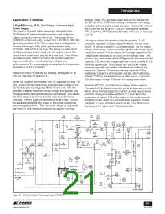
A High Efficiency, 150 W, 250 – 380 VDC Input
Power Supply
The circuit shown in Figure 42 delivers 150 W (19 V @ 7.7 A) at
84% efficiency using a TOP258Y from a 250 VDC to 380 VDC
input. A DC input is shown, as typically at this power level a
power factor correction stage would precede this supply,
providing the DC input. Capacitor C1 provides local decoupling,
necessary when the supply is remote from the main PFC output
capacitor.
The secondary is rectified and smoothed by D2, D3 and C5,
C6, C7 and C8. Two windings are used and rectified with
separate diodes D2 and D3 to limit diode dissipation. Four
capacitors are used to ensure their maximum ripple current
specification is not exceeded. Inductor L1 and capacitors C15
and C16 provide switching noise filtering.
The flyback topology is still usable at this power level due to the
high output voltage, keeping the secondary peak currents low
enough so that the output diode and capacitors are reasonably
sized. In this example, the TOP258YN is at the upper limit of its
power capability.
Output voltage is controlled using a TL431 reference IC and
R15, R16 and R17 to form a potential divider to sense the
output voltage. Resistor R12 and R24 together limit the
optocoupler LED current and set overall control loop DC gain.
Control loop compensation is achieved using components C12,
C13, C20 and R13. Diode D6, resistor R23 and capacitor C19
form a soft finish network. This feeds current into the control
pin prior to output regulation, preventing output voltage
overshoot and ensuring startup under low line, full load
conditions.
Resistors R3, R6 and R7 provide output power limiting,
maintaining relatively constant overload power with input voltage.
Line sensing is implemented by connecting a 4 MΩ resistor from
the V pin to the DC rail. Resistors R4 and R5 together form the
4 MΩ line sense resistor. If the DC input rail rises above
450 VDC, then TOPSwitch-HX will stop switching until the
voltage returns to normal, preventing device damage.
Due to the high primary current, a low leakage inductance
transformer is essential. Therefore, a sandwich winding with a
copper foil secondary was used. Even with this technique, the
leakage inductance energy is beyond the power capability of a
simple Zener clamp. Therefore, R1, R2 and C3 are added in
parallel to VR1 and VR3, two series TVS diodes being used to
reduce dissipation. During normal operation, very little power is
Sufficient heat sinking is required to keep the TOPSwitch-HX
device below 110 °C when operating under full load, low line
and maximum ambient temperature. Airflow may also be
required if a large heat sink area is not acceptable.
2.2 nF
C14
47 pF
1 kV
R14
250 VAC
22
7
C4
R2
68 k7
2 W
R1
68 k7
2 W
0.5 W
250 - 380
C5-C8
820 MF
25 V
C15-C16
820 MF
25 V
VDC
+19 V,
7.7 A
L1
1
4
13,14
F1
RT1
5 7
C3
4.7 nF
1 kV
tO
3.3 MH
4 A
R6
4.7 M
R4
D2
7
2.0 M7
MBR20100CT
11
12
D1
BYV26C
D3
RTN
R7
4.7 M
R5
2.0 -7
MBR20100CT
7
VR1, VR3
P6KE100A
9,10
7
D4
1N4148
5
C1
22 MF
400 V
R18
C17
22 7
47 pF
R20
1.5 k7
2 W
0.5 W
1 kV
C20
T1
EI35
R12
R8
4.7
1.0 MF
240 7
7
50 V
0.125 W
C9
10 MF
D5
1N4937
R24
VR2
1N5258B
36 V
50 V
30 7
R21
1.5 k7
2 W
0.125 W
R16
31.6 k7
1%
R19
4.7 7
R23
15 k7
U2
PC817A
0.125 W
R11
TOPSwitch-HX
U1
TOP258YN
R17
562 7
1%
C12
4.7 nF
50 V
1 k7
0.125 W
D
V
R22
1.5 k7
2 W
CONTROL
U2
PC817B
C
C13
100 nF
50 V
R13
56 k7
R10
0.125 W
S
X
F
D6
1N4148
6.8 7
C11
100 nF
50 V
C19
10 MF
R3
8.06 k7
1%
C18
120 pF
1 kV
C10
50 V
U3
TL431
2%
R15
47 MF
10 V
4.75 k7
1%
PI-4795-092007
Figure 42. 150 W, 19 V Power Supply using TOP258YN.
22
Rev. F 01/09
www.powerint.com

 POWERINT [ Power Integrations ]