TOP252-262
A High Efficiency, 65 W, Universal Input Power Supply
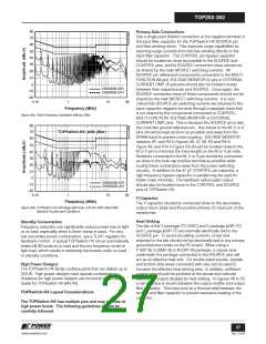
The circuit shown in Figure 44 delivers 65 W (19 V @ 3.42 A) at
88% efficiency using a TOP260EN operating over an input
voltage range of 90 VAC to 265 VAC.
The secondary output from the transformer is rectified by diode
D2 and filtered by capacitors C13 and C14. Ferrite Bead L3 and
capacitors C15 form a second stage filter and effectively reduce
the switching noise to the output.
Capacitors C1 and C6 and inductors L1 and L2 provide
common mode and differential mode EMI filtering. Capacitor C2
is the bulk filter capacitor that ensures low ripple DC input to the
flyback converter stage. Capacitor C4 provides decoupling for
switching currents reducing differential mode EMI.
Output voltage is controlled using a LM431 reference IC.
Resistor R19 and R20 form a potential divider to sense the
output voltage. Resistor R16 limits the optocoupler LED current
and sets the overall control loop DC gain. Control loop
compensation is achieved using C18 and R21. The components
connected to the control pin on the primary side C8, C9 and
R15 set the low frequency pole and zero to further shape the
control loop response. Capacitor C17 provides a soft finish
during startup. Optocoupler U2 is used for isolation of the
feedback signal.
In this example, the TOP260EN is used at reduced current limit
to improve efficiency.
Resistors R5, R6 and R7 provide power limiting, maintaining
relatively constant overload power with input voltage. Line
sensing is implemented by connecting a 4 MΩ impedance from
the V pin to the DC rail. Resistors R3 and R4 together form the
4 MΩ line sense resistor. If the DC input rail rises above
450 VDC, then TOPSwitch-HX will stop switching until the
voltage returns to normal, preventing device damage.
Diode D4 and capacitor C10 form the bias winding rectifier and
filter. Should the feedback loop break due to a defective
component, a rising bias winding voltage will cause the zener
VR2 to break down and trigger the over voltage protection
which will inhibit switching.
This circuit features a high efficiency clamp network consisting
of diode D1, zener VR1, capacitor C5 together with resistors R8
and R9. The snubber clamp is used to dissipate the energy of
the leakage reactance of the transformer. At light load levels,
very little power is dissipated by VR1 improving efficiency as
compared to a conventional RCD clamp network.
An optional secondary side over voltage protection feature
which offers higher precision (as compared to sensing via the
bias winding) is implemented using VR3, R18 and U3. Excess
voltage at the output will cause current to flow through the
optocoupler U3 LED which in turn will inject current in the V-pin
through resistor R13, thereby triggering the over voltage
protection feature.
C6
C12
1 nF
100 V
2.2 nF
R16
33 7
250 VAC
L3
Ferrite
Bead
C5
C13
470 MF 470 MF
25 V 25 V
C14
C15
47 MF
25 V
VR1
2.2 nF
T1
BZY97C180
19 V, 3.42 A
1 kV
RM10
180 V
4
5
6
FL1
D2
MBR20100CT
3KBP08M
BR1
FL2
R8
R9
RTN
100 7
1 k7
C10
22 MF
50 V
VR2
R10
1N5248B
18 V
VR3
BZX79-C22
22 V
73.2 k7
R3
R5
3
2
2.0 M7 5.1 M7
C11
D1
100 nF
DL4937
50 V
R11
D4 BAV19WS
L1
2 M7
12 mH
R16
R18
47 7
R4
R6
680 7
2.0 M7 6.8 M7
R12
5.1 k7
C7
100 nF
25 V
C2
120 MF
400 V
D5
U3B
BAV19WS
PC357A
R1
R2
2.2 M7 2.2 M7
U3A
PC357A
C4
100 nF
400 V
D3
BAV19WS
U2A
C1
LTY817C
F1
4 A
330 nF
275 VAC
U2B
LTY817C
R13
5.1 7
TOPSwitch-HX
U1
D
S
V
TOP260EN
L
E
N
R14
100 7
D6
1N4148
CONTROL
R19
C
68.1 k7
C18
100 nF
R15
X
F
6.8 7
C16
90 - 265
VAC
R21
1 k7
1 MF
C8
100 nF
50 V
R7
15 k7
1%
C9
47 MF
16 V
50 V
C3
470 pF
250 VAC
C17
33 MF
35 V
U4
LM431
2%
R20
10 k7
L2
Ferrite Bead
PI-4998-021408
Figure 44. 65 W, 19 V Power Supply Using TOP260EN.
24
Rev. F 01/09
www.powerint.com

 POWERINT [ Power Integrations ]