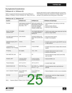
TOP252-262
winding. Zener VR2 will break down and current will flow into
the “M” pin of the TOPSwitch initiating a hysteretic overvoltage
protection with automatic restart attempts. Resistor R5 will limit
the current into the M pin to < 336 μA, thus setting hysteretic
OVP. If latching OVP is desired, the value of R5 can be reduced
to 20 Ω.
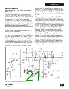
Application Examples
A High Efficiency, 35 W, Dual Output - Universal Input
Power Supply
The circuit in Figure 41 takes advantage of several of the
TOPSwitch-HX features to reduce system cost and power
supply size and to improve efficiency. This design delivers
35 W total continuous output power from a 90 VAC to 265 VAC
input at an ambient of 50 ºC in an open frame configuration. A
nominal efficiency of 84% at full load is achieved using
TOP258P. With a DIP-8 package, this design provides 35 W
continuous output power using only the copper area on the
circuit board underneath the part as a heat sink. The different
operating modes of the TOPSwitch-HX provide significant
improvement in the no-load, standby, and light load
performance of the power supply as compared to the previous
generations of the TOPSwitch.
The output voltage is controlled using the amplifier TL431.
Diode D9, capacitor C20 and resistor R16 form the soft finish
circuit. At startup, capacitor C20 is discharged. As the output
voltage starts rising, current flows through the optocoupler diode
inside U2A, resistor R13 and diode D9 to charge capacitor C20.
This provides feedback to the circuit on the primary side. The
current in the optocoupler diode U2A gradually decreases as the
capacitor C20 becomes charged and the control amplifier IC U3
becomes operational. This ensures that the output voltage
increases gradually and settles to the final value without any
overshoot. Resistor R16 ensures that the capacitor C20 is
maintained charged at all times after startup, which effectively
isolates C20 from the feedback circuit after startup. Capacitor
C20 discharges through R16 when the supply shuts down.
Resistors R3 and R4 provide line sensing, setting line UV at
100 VDC and line OV at 450 VDC.
Diode D5, together with resistors R6, R7, capacitor C6 and TVS
VR1, forms a clamp network that limits the drain voltage of the
TOPSwitch after the integrated MOSFET turns off. TVS VR1
provides a defined maximum clamp voltage and typically only
conducts during fault conditions such as overload. This allows
the RCD clamp (R6, R7, C6 and D5) to be sized for normal
operation, thereby maximizing efficiency at light load. Should
the feedback circuit fail, the output of the power supply may
exceed regulation limits. This increased voltage at output will
also result in an increased voltage at the output of the bias
Resistors R20, R21 and R18 form a voltage divider network.
The output of this divider network is primarily dependent on the
divider circuit formed using R20 and R21 and will vary to some
extent for changes in voltage at the 15 V output due to the
connection of resistor R18 to the output of the divider network.
Resistor R19 and Zener VR3 improve cross regulation in case
only the 5 V output is loaded, which results in the 15 V output
operating at the higher end of the specification.
C7
C12
470 pF
100 V
R11
33 7
C6
2.2 nF
3.9 nF
250 VAC
1 kV
C13
680 MF
25 V
C14
680 MF
25 V
C15
220 MF
25 V
D7
SB560
L2
T1
EER28
R6
3.3 MH
+12 V,
2 A
22 k7
2
7
2 W
VR1
C16
470 pF
100 V
C18
220 MF
10 V
D1
1N4937
D2
1N4007
R12
33 7
L3
3.3 MH
P6KE200A
RTN
3
11
+5 V,
2.2 A
D8
R7
SB530
20 7
1/2 W
4
9
6
RTN
C17
C10
2200 MF
10 MF
10 V
C11
2.2 nF
250 VAC
D5
FR106
R10
4.7 7
50 V
R3
2.0 M7
D3
1N4937
D4
1N4007
D6
R19
10 7
FR106
5
L1
6.8 mH
R4
2.0 M7
VR3
R14
BZX55B8V2
8.2 V
22 7
R13
330 7
C4
100 MF
400 V
2%
C19
1.0 MF
50 V
R1
R2
VR2
1N5250B
20 V
1 M7 1 M7
R5
5.1 k7
C3
220 nF
275 VAC
R15
1 k7
F1
3.15 A
U2B
PS2501-
1-H-A
U2A
TOPSwitch-HX
PS2501-
1-H-A
tO
R18
196 k7
1%
R20
RT1
10 7
D
M
U1
L
E
N
TOP258PN
C
12.4 k7
CONTROL
1%
R17
10 k7
R16
10 k7
D9
1N4148
R8
S
6.8 7
C8
100 nF
50 V
90 - 265
VAC
C21
220 nF
50 V
C9
47 MF
16 V
C20
10 MF
50 V
U3
TL431
2%
R21
10 k7
1%
PI-4747-020508
Figure 41. 35 W Dual Output Power Supply using TOP258PN.
21
www.powerint.com
Rev. F 01/09

 POWERINT [ Power Integrations ]