TOP252-262
TOPSwitch-HX Design Considerations
heat sinking, air circulation, etc.). The higher DCMAX of
TOPSwitch-HX, along with an appropriate transformer turns
ratio, can allow the use of a 80 V Schottky diode for higher
efficiency on output voltages as high as 15 V (see Figure 41).
Power Table
The data sheet power table (Table 1) represents the maximum
practical continuous output power based on the following
conditions:
Bias Winding Capacitor
1. 12 V output.
Due to the low frequency operation at no-load, a 10 μF bias
winding capacitor is recommended.
2. Schottky or high efficiency output diode.
3. 135 V reflected voltage (VOR) and efficiency estimates.
4. A 100 VDC minimum for 85-265 VAC and 250 VDC mini-
mum for 230 VAC.
5. Sufficient heat sinking to keep device temperature ≤100 °C.
6. Power levels shown in the power table for the M/P package
device assume 6.45 cm2 of 610 g/m2 copper heat sink area
in an enclosed adapter, or 19.4 cm2 in an open frame.
Soft-Start
Generally, a power supply experiences maximum stress at
start-up before the feedback loop achieves regulation. For a
period of 17 ms, the on-chip soft-start linearly increases the
drain peak current and switching frequency from their low
starting values to their respective maximum values. This
causes the output voltage to rise in an orderly manner, allowing
time for the feedback loop to take control of the duty cycle.
This reduces the stress on the TOPSwitch-HX MOSFET, clamp
circuit and output diode(s), and helps prevent transformer
saturation during start-up. Also, soft-start limits the amount of
output voltage overshoot and, in many applications, eliminates
the need for a soft-finish capacitor.
The provided peak power depends on the current limit for the
respective device.
TOPSwitch-HX Selection
Selecting the optimum TOPSwitch-HX depends upon required
maximum output power, efficiency, heat sinking constraints,
system requirements and cost goals. With the option to
externally reduce current limit, an Y, E/L or M package
TOPSwitch-HX may be used for lower power applications
where higher efficiency is needed or minimal heat sinking is
available.
EMI
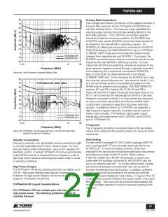
The frequency jitter feature modulates the switching frequency
over a narrow band as a means to reduce conducted EMI peaks
associated with the harmonics of the fundamental switching
frequency. This is particularly beneficial for average detection
mode. As can be seen in Figure 45, the benefits of jitter increase
with the order of the switching harmonic due to an increase in
frequency deviation. Devices in the P, G or M package and
TOP259-261YN operate at a nominal switching frequency of
66 kHz. The FREQUENCY pin of devices in the TOP254-258 Y
and E packages offer a switching frequency option of 132 kHz or
66 kHz. In applications that require heavy snubber on the drain
node for reducing high frequency radiated noise (for example,
video noise sensitive applications such as VCRs, DVDs, monitors,
TVs, etc.), operating at 66 kHz will reduce snubber loss, resulting
in better efficiency. Also, in applications where transformer size is
not a concern, use of the 66 kHz option will provide lower EMI
and higher efficiency. Note that the second harmonic of 66 kHz
is still below 150 kHz, above which the conducted EMI
specifications get much tighter. For 10 W or below, it is possible
to use a simple inductor in place of a more costly AC input
common mode choke to meet worldwide conducted EMI limits.
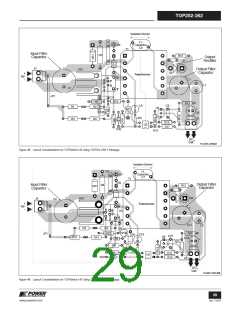
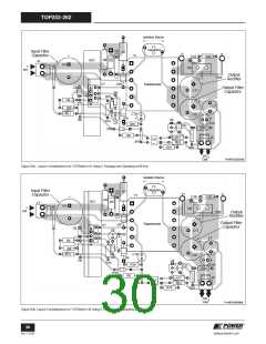
Input Capacitor
The input capacitor must be chosen to provide the minimum
DC voltage required for the TOPSwitch-HX converter to
maintain regulation at the lowest specified input voltage and
maximum output power. Since TOPSwitch-HX has a high
DCMAX limit and an optimized dual slope line feed forward for
ripple rejection, it is possible to use a smaller input capacitor.
For TOPSwitch-HX, a capacitance of 2 μF per watt is possible
for universal input with an appropriately designed transformer.
Primary Clamp and Output Reflected Voltage VOR
A primary clamp is necessary to limit the peak TOPSwitch-HX
drain to source voltage. A Zener clamp requires few parts and
takes up little board space. For good efficiency, the clamp
Zener should be selected to be at least 1.5 times the output
reflected voltage VOR, as this keeps the leakage spike
conduction time short. When using a Zener clamp in a
universal input application, a VOR of less than 135 V is
recommended to allow for the absolute tolerances and
temperature variations of the Zener. This will ensure efficient
operation of the clamp circuit and will also keep the maximum
drain voltage below the rated breakdown voltage of the
TOPSwitch-HX MOSFET. A high VOR is required to take full
advantage of the wider DCMAX of TOPSwitch-HX. An RCD
clamp provides tighter clamp voltage tolerance than a Zener
clamp and allows a VOR as high as 150 V. RCD clamp
dissipation can be minimized by reducing the external current
limit as a function of input line voltage (see Figures 23 and 36).
The RCD clamp is more cost effective than the Zener clamp but
requires more careful design (see Quick Design Checklist).
Transformer Design
It is recommended that the transformer be designed for
maximum operating flux density of 3000 Gauss and a peak flux
density of 4200 Gauss at maximum current limit. The turns
ratio should be chosen for a reflected voltage (VOR) no greater
than 135 V when using a Zener clamp or 150 V (max) when
using an RCD clamp with current limit reduction with line
voltage (overload protection). For designs where operating
current is significantly lower than the default current limit, it is
recommended to use an externally set current limit close to the
operating peak current to reduce peak flux density and peak
power (see Figures 22 and 35). In most applications, the tighter
current limit tolerance, higher switching frequency and soft-start
features of TOPSwitch-HX contribute to a smaller transformer
when compared to TOPSwitch-GX.
Output Diode
The output diode is selected for peak inverse voltage, output
current, and thermal conditions in the application (including
26
Rev. F 01/09
www.powerint.com

 POWERINT [ Power Integrations ]