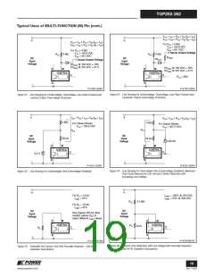
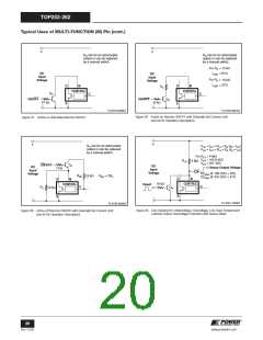
TOP252-262
TOPSwitch-HX and R20, C9, R22 and VR5. Should the bias
winding output voltage across C13 rise due to output overload
or an open loop fault (opto coupler failure), then VR5 conducts
triggering the latching shutdown. To prevent false triggering
due to short duration overload, a delay is provided by R20, R22
and C9.
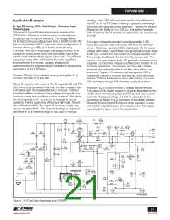
A High Efficiency, 20 W continuous – 80 W Peak, Universal
Input Power Supply
The circuit shown in Figure 43 takes advantage of several of
TOPSwitch-HX features to reduce system cost and power
supply size and to improve power supply efficiency while
delivering significant peak power for a short duration. This
design delivers continuous 20 W and peak 80 W at 32 V from
an 90 VAC to 264 VAC input. A nominal efficiency of 82% at full
load is achieved using TOP258MN. The M-package part has an
optimized current limit to enable design of power supplies
capable of delivering high power for a short duration.
To reset the supply following a latching shutdown, the V pin
must fall below the reset threshold. To prevent the long reset
delay associated with the input capacitor discharging, a fast AC
reset circuit is used. The AC input is rectified and filtered by
D13 and C30. While the AC supply is present, Q3 is on and Q1
is off, allowing normal device operation. However when AC is
removed, Q1 pulls down the V pin and resets the latch. The supply
will then return to normal operation when AC is again applied.
Resistor R12 sets the current limit of the part. Resistors R11
and R14 provide line feed forward information that reduces the
current limit with increasing DC bus voltage, thereby maintaining
a constant overload power level with increasing line voltage.
Resistors R1 and R2 implement the line undervoltage and over-
voltage function and also provide feed forward compensation for
reducing line frequency ripple at the output. The overvoltage
feature inhibits TOPSwitch-HX switching during a line surge
extending the high voltage withstand to 700 V without device
damage.
Transistor Q2 provides an additional lower UV threshold to the
level programmed via R1, R2 and the V pin. At low input AC
voltage, Q2 turns off, allowing the X pin to float and thereby
disabling switching.
A simple feedback circuit automatically regulates the output
voltage. Zener VR3 sets the output voltage together with the
voltage drop across series resistor R8, which sets the DC gain
of the circuit. Resistors R10 and C28 provide a phase boost to
improve loop bandwidth.
The snubber circuit comprising of VR7, R17, R25, C5 and D2
limits the maximum drain voltage and dissipates energy stored in
the leakage inductance of transformer T1. This clamp
configuration maximizes energy efficiency by preventing C5 from
discharging below the value of VR7 during the lower frequency
operating modes of TOPSwitch-HX. Resistor R25 damps high
frequency ringing for reduced EMI.
Diodes D6 and D7 are low-loss Schottky rectifiers, and
capacitor C20 is the output filter capacitor. Inductor L3 is a
common mode choke to limit radiated EMI when long output
cables are used and the output return is connected to safety
earth ground. Example applications where this occurs include
PC peripherals, such as inkjet printers.
A combined output overvoltage and over power protection
circuit is provided via the latching shutdown feature of
C8
1 nF
250 VAC
R19 C26
68 100 pF
0.5 W 1 kV
7
C31
C20
330
50 V
32 V
625 mA, 2.5 APK
M
F
22
M
F
L2
50 V
L3
1
2
3
10
3.3
M
H
D6-D7
D8
1N4007
D9
1N4007
VR7
BZY97C150
150 V
RTN
STPS3150
9
5
R25
C3
120
400 V
47 MH
100
7
MF
C29
220 nF
50 V
o
C13
t
R11
10
M
F
R1
2 M
NC
C10
R17
RT1
10
3.6 M7
50 V
D11
D10
7
C5
10 nF
1 kV
1 nF
1 k
7
4
1N4007
1N4007
7
250 VAC
0.5 W
D5
T1
EF25
LL4148
R10
56
7
R8
1.5 k
L1
7
D2
FR107
5.3 mH
R2
2 M
R14
C28
330 nF
50 V
7
3.6 M7
D13
1N4007
R24
R23
VR3
1N5255B
28 V
1 M
7
1 M
7
U2A
PC817D
VR5
1N5250B
20 V
R20
130 k
C9
R3
2 M
7
R22
1 MF
7
V
D
S
100 V
2 M
7
C1
F1
3.15 A
R21
220 nF
CONTROL
R9
275 VAC
1 M
7
2 k
7
R4
2 M
0.125 W
7
C
PI-4833-092007
90 - 264
VAC
X
R15
1 k
7
R6
6.8 7
TOPSwitch-HX
U4
TOP258MN
R12
7.5 k
1%
C6
100 nF
50 V
Q1
2N3904
7
C30
100 nF
Q2
2N3904
400 V
Q3
2N3904
C7
47
16 V
MF
R26
68 k
R18
39 k
7
7
Figure 43. 20 W Continuous, 80 W Peak, Universal Input Power Supply using TOP258MN.
23
www.powerint.com
Rev. F 01/09

 POWERINT [ Power Integrations ]