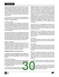
TOP242-250
Output Filter Capacitors
Solder Side
Safety Spacing
Component Side
Y1-
+
Capacitor
TOP VIEW
HV
T
r
a
n
s
f
o
r
m
e
r
PRI
PRI
Input Filter
Capacitor
SEC
-
R1a - 1c
BIAS
D
S
X
L
DC
Out
-
+
C
Opto-
coupler
Maximize hatched copper
areas (
) for optimum
heat sinking
TOPSwitch-GX
PI-2734-043001
Figure 49. Layout Considerations for TOPSwitch-GX using R Package.
3. Thermal check – At maximum output power, minimum
input voltage and maximum ambient temperature, verify
that temperature specifications are not exceeded for
TOPSwitch-GX, transformer, output diodes and output
capacitors. Enough thermal margin should be allowed for
the part-to-part variation of the RDS(ON) of TOPSwitch-GX,
as specified in the data sheet. The margin required can
either be calculated from the tolerances or it can be
accounted for by connecting an external resistance in
series with the DRAIN pin and attached to the same
heatsink, having a resistance value that is equal to the
difference between the measured RDS(ON) of the device
under test and the worst case maximum specification.
Quick Design Checklist
As with any power supply design, all TOPSwitch-GX designs
should be verified on the bench to make sure that components
specificationsarenotexceededunderworstcaseconditions.The
following minimum set of tests is strongly recommended:
1. Maximum drain voltage – Verify that peak VDS does not
exceed 675 V at highest input voltage and maximum
overload output power. Maximum overload output power
occurswhentheoutputisoverloadedtoaleveljustbeforethe
power supply goes into auto-restart (loss of regulation).
2. Maximumdraincurrent–Atmaximumambienttemperature,
maximum input voltage and maximum output load, verify
drain current waveforms at start-up for any signs of
transformer saturation and excessive leading edge current
spikes. TOPSwitch-GX has a leading edge blanking time of
220 ns to prevent premature termination of the ON-cycle.
Verify that the leading edge current spike is below the
allowed current limit envelope (see Figure 52) for the
drain current waveform at the end of the 220 ns blanking
period.
Design Tools
For a discussion on utilizing TOPSwitch-GX in a forward
converter configuration, please refer to the TOPSwitch-GX
Forward Design Methodology Application Note.
Up-to-date information on design tools can be found at the
Power Integrations website: www.powerint.com
M
32 12/04

 POWERINT [ Power Integrations ]