TOP242-250
SOURCE connection trace should not be shared by the main
MOSFET switching currents. All SOURCE pin referenced
components connected to the MULTI-FUNCTION, LINE-
SENSE or EXTERNAL CURRENT LIMIT pins should
also be located closely between their respective pin and
SOURCE. Once again, the SOURCE connection trace of these
components should not be shared by the main MOSFET
switching currents. It is very critical that SOURCE pin
switching currents are returned to the input capacitor negative
terminal through a seperate trace that is not shared by the
components connected to CONTROL, MULTI-FUNCTION,
LINE-SENSE or EXTERNAL CURRENT LIMIT pins. This
is because the SOURCE pin is also the controller ground
reference pin.
frequency radiated noise (for example, video noise sensitive
applications such as VCR, DVD, monitor, TV, etc.), operating
at 66 kHz will reduce snubber loss resulting in better efficiency.
Also, in applications where transformer size is not a concern,
use of the 66 kHz option will provide lower EMI and higher
efficiency. Note that the second harmonic of 66 kHz is still
below 150 kHz, above which the conducted EMI specifications
get much tighter.
For 10 W or below, it is possible to use a simple inductor in
place of a more costly AC input common mode choke to meet
worldwide conducted EMI limits.
Transformer Design
It is recommended that the transformer be designed for
maximum operating flux density of 3000 Gauss and a peak flux
densityof4200Gaussatmaximumcurrentlimit. Theturnsratio
should be chosen for a reflected voltage (VOR) no greater than
135 V when using a Zener clamp, or 150 V (max) when using
an RCD clamp with current limit reduction with line voltage
(overload protection).
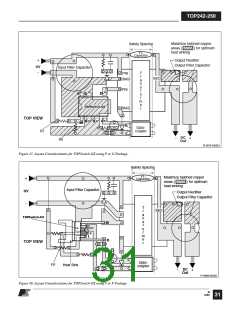
Any traces to the M, L or X pins should be kept as short as
possible and away from the DRAIN trace to prevent noise
coupling. LINE-SENSE resistor (R1 in Figures 47-49) should
be located close to the M or L pin to minimize the trace length
on the M or L pin side.
In addition to the 47 µF CONTROL pin capacitor, a high
frequency bypass capacitor in parallel may be used for better
noise immunity. The feedback optocoupler output should
also be located close to the CONTROL and SOURCE pins of
TOPSwitch-GX.
For designs where operating current is significantly lower than
the default current limit, it is recommended to use an externally
setcurrentlimitclosetotheoperatingpeakcurrenttoreducepeak
flux density and peak power (see Figures 20 and 34). In most
applications,thetightercurrentlimittolerance,higherswitching
frequency and soft-start features of TOPSwitch-GX contribute
to a smaller transformer when compared to TOPSwitch-II.
Y-Capacitor
The Y-capacitor should be connected close to the secondary
output return pin(s) and the positive primary DC input pin of
the transformer.
Standby Consumption
Frequency reduction can significantly reduce power loss at
light or no load, especially when a Zener clamp is used. For
very low secondary power consumption, use aTL431 regulator
for feedback control. Alternately, switching losses can be
significantly reduced by changing from 132 kHz in normal
operation to 66 kHz under light load conditions.
Heat Sinking
The tab of the Y package (TO-220) or F package (TO-262)
is internally electrically tied to the SOURCE pin. To avoid
circulating currents, a heat sink attached to the tab should not
be electrically tied to any primary ground/source nodes on the
PC board.
TOPSwitch-GX Layout Considerations
When using a P (DIP-8), G (SMD-8) or R (TO-263) package,
a copper area underneath the package connected to the
SOURCE pins will act as an effective heat sink. On double
sided boards (Figure 49), top side and bottom side areas
connected with vias can be used to increase the effective heat
sinking area.
As TOPSwitch-GX has additional pins and operates at
muchhigherpowerlevelscomparedtopreviousTOPSwitch
families, the following guidelines should be carefully
followed.
Primary Side Connections
In addition, sufficient copper area should be provided at
the anode and cathode leads of the output diode(s) for heat
sinking.
Use a single point (Kelvin) connection at the negative terminal
of the input filter capacitor for the TOPSwitch-GX SOURCE
pin and bias winding return. This improves surge capabilities
by returning surge currents from the bias winding directly to
the input filter capacitor.
In Figures 47, 48 and 49, a narrow trace is shown between
the output rectifier and output filter capacitor. This trace acts
as a thermal relief between the rectifier and filter capacitor to
prevent excessive heating of the capacitor.
The CONTROL pin bypass capacitor should be located as
close as possible to the SOURCE and CONTROL pins and its
M
30 12/04

 POWERINT [ Power Integrations ]