TOP242-250
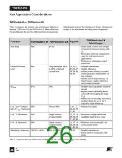
Function
TOPSwitch-GX
TOPSwitch-FX TOPSwitch-GX
Advantages
Light Load Operation Cycle skipping
Frequency and duty
cycle reduction
• Improves light load efficiency
• Reduces no-load consumption
Line Sensing/Exter-
nally Set Current
Limit (Y, R and F
Packages)
Line sensing and
externally set current
limit mutually
Line sensing and
• Additional design flexibility allows all
features to be used simultaneously
externally set current
limit possible simul-
taneously (functions
split onto L and X pins
exclusive (M pin)
Current Limit
Programming Range
100% to 40%
100% to 30%
• Minimizes transformer core size in highly
continuous designs
P/G Package Current Identical to Y
TOP243-246 P and
G packages internal
• Matches device current limit to package
dissipation capability
Limits
package
current limits reduced • Allows more continuous design to lower
device dissipation (lower RMS currents)
Y/R/F Package
Current Limits
100% (R and F
package N/A*)
90% (for equivalent
RDS(ON)
• Minimizes transformer core size
• Optomizes efficiency for most
applications
)
Thermal Shutdown
125 °C min.
70 °C hysteresis
130 °C min.
75 °C hysteresis
• Allows higher output powers in high
ambient temperature applications
90 µA
60 µA
• Reduces output line frequency ripple at
low line
• DCMAX reduction optimized for forward
design
Maximum Duty Cycle
Reduction Threshold
Line Under-Voltage
Negative (turn-off)
Threshold
N/A*
40% of positive
(turn-on) threshold
• Provides a well defined turn-off threshold
as the line voltage falls
Soft-Start
10 ms (duty cycle)
10 ms (duty cycle +
current limit)
• Gradually increasing current limit in
addition to duty cycle during soft-start
further reduces peak current and voltage
• Further reduces component stresses
during start up
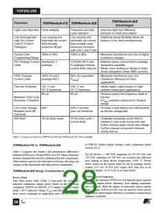
Table 5. Comparison Between TOPSwitch-FX and TOPSwitch-GX. *Not available
to TOP250: Higher output voltages, with a maximum output
current of 6 A.
TOPSwitch-FX vs. TOPSwitch-GX
Table 5 compares the features and performance differences
between TOPSwitch-GX and TOPSwitch-FX. Many of the new
features eliminate the need for additional discrete components.
Other features increase the robustness of design, allowing cost
savings in the transformer and other power components.
For all devices, a 100 VDC minimum for 85-265 VAC and
250 VDC minimum for 230 VAC are assumed and sufficient
heat sinking to keep device temperature ≤100 °C. Power
levels shown in the power table for the R package device
assume 6.45 cm2 of 610 g/m2 copper heat sink area in an
enclosed adapter, or 19.4 cm2 in an open frame.
TOPSwitch-GX Design Considerations
TOPSwitch-GX Selection
Power Table
Selecting the optimum TOPSwitch-GX depends upon required
maximum output power, efficiency, heat sinking constraints
and cost goals. With the option to externally reduce current
limit, a larger TOPSwitch-GX may be used for lower power
applications where higher efficiency is needed or minimal heat
sinking is available.
Data sheet power table (Table 1) represents the maximum
practical continuous output power based on the following
conditions: TOP242 to TOP246: 12 V output, Schottky output
diode, 150 V reflected voltage (VOR) and efficiency estimates
from curves contained in application note AN-29. TOP247
M
28 12/04

 POWERINT [ Power Integrations ]