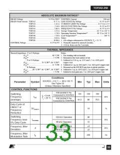
TOP242-250
Input Capacitor
transformersaturationduringstart-up. Also,soft-startlimitsthe
amount of output voltage overshoot and, in many applications,
eliminates the need for a soft-finish capacitor.
Theinputcapacitormustbechosentoprovidetheminimum DC
voltage required for the TOPSwitch-GX converter to maintain
regulation at the lowest specified input voltage and maximum
output power. Since TOPSwitch-GX has a higher DCMAX than
TOPSwitch-II, it is possible to use a smaller input capacitor.
ForTOPSwitch-GX,acapacitanceof2µFperwattispossiblefor
universal input with an appropriately designed transformer.
EMI
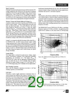
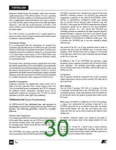
The frequency jitter feature modulates the switching frequency
over a narrow band as a means to reduce conducted EMI peaks
associated with the harmonics of the fundamental switching
frequency. This is particularly beneficial for average detection
mode. As can be seen in Figure 46, the benefits of jitter increase
with the order of the switching harmonic due to an increase in
frequency deviation.
Primary Clamp and Output Reflected Voltage VOR
Aprimary clamp is necessary to limit the peak TOPSwitch-GX
drain to source voltage. A Zener clamp requires few parts and
takes up little board space. For good efficiency, the clamp
Zener should be selected to be at least 1.5 times the output
reflectedvoltageVOR,asthiskeepstheleakagespikeconduction
time short. When using a Zener clamp in a universal input
application, a VOR of less than 135 V is recommended to allow
for the absolute tolerances and temperature variations of the
Zener. This will ensure efficient operation of the clamp circuit
and will also keep the maximum drain voltage below the rated
breakdown voltage of the TOPSwitch-GX MOSFET.
The FREQUENCY pin of TOPSwitch-GX offers a switching
frequency option of 132 kHz or 66 kHz. In applications that
require heavy snubbers on the drain node for reducing high
80
70
60
50
40
30
20
-10
0
TOPSwitch-II (no jitter)
AhighVOR isrequiredtotakefulladvantageofthewiderDCMAX
of TOPSwitch-GX. An RCD clamp provides tighter clamp
voltage tolerance than a Zener clamp and allows a VOR as high
as150V. RCDclampdissipationcanbeminimizedbyreducing
the external current limit as a function of input line voltage (see
Figures 21 and 35). The RCD clamp is more cost effective than
the Zener clamp but requires more careful design (see Quick
Design Checklist).
EN55022B (QP)
EN55022B (AV)
-10
-20
0.15
1
10
30
Output Diode
Frequency (MHz)
The output diode is selected for peak inverse voltage, output
current, and thermal conditions in the application (including
heatsinking, air circulation, etc.). The higher DCMAX of
TOPSwitch-GX, along with an appropriate transformer turns
ratio, can allow the use of a 60 V Schottky diode for higher
efficiency on output voltages as high as 15 V (see Figure 41: A
12 V, 30 W design using a 60 V Schottky for the output diode).
Figure 46a. TOPSwitch-II Full Range EMI Scan (100 kHz, No
Jitter).
80
70
60
TOPSwitch-GX (with jitter)
50
40
30
20
-10
0
Bias Winding Capacitor
Due to the low frequency operation at no-load a 1 µF bias
winding capacitor is recommended.
Soft-Start
Generally, a power supply experiences maximum stress at
start-up before the feedback loop achieves regulation. For a
periodof10ms,theon-chipsoft-startlinearlyincreasestheduty
cycle from zero to the default DCMAX at turn on. In addition,
the primary current limit increases from 85% to 100% over the
same period. This causes the output voltage to rise in an orderly
manner, allowing time for the feedback loop to take control of
the duty cycle. This reduces the stress on the TOPSwitch-GX
MOSFET, clamp circuit and output diode(s), and helps prevent
EN55022B (QP)
EN55022B (AV)
-10
-20
0.15
1
10 30
Frequency (MHz)
Figure 46b. TOPSwitch-GX Full Range EMI Scan (132 kHz, With
Jitter) with Identical Circuitry and Conditions.
M
12/04
29

 POWERINT [ Power Integrations ]