RELEASED
PM7350 S/UNI DUPLEX
DATA SHEET
PMC-1980581
ISSUE 8
DUAL SERIAL LINK PHY MULTIPLEXER
00001
00010
00011
00100
00101
00110
00111
ACT_RCLK
SYSCLK
CSDCLK
DCLK
CCLK
L1_RCLK
L2_RCLK
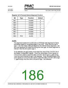
SELOCD:
The SELOCD bit allows usage of the OCD signal instead of the LCD signal to
gate to gate the ACTIVEBIT extracted from the high-speed serial links. This is
useful to speed up simulation, LCD being a very slow signal.
LINKSELBP:
The LINKSELBP allows to bypass the sequenced automatic link selection
circuit. When LINKSELBP is set to logic 1, the high-speed serial link selection
is immediate. When set to logic 0, the high-speed serial link selection will be
performed prior just prior to an incoming cell (idle or data) on the “to be
active” serial link.
TCADIS:
The TCADIS bit disables the transmission of the flow control information in
the upstream direction of the inactive high-speed serial link. Its usage is
intended for test purposes. When set to logic 1, the S/UMI-DUPLEX will
indicates on the inactive high-speed serial link that it can not accept cells on
any logical channel. When set to logic 0, the flow control bits for the logical
channel are identical to the flow control bits of the active channel. The flow
control bits of the active high-speed serial link are not affected by the
TCADIS.
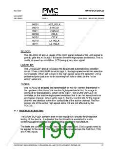
11.1 RAM Built-In-Self-Test
The S/UNI-DUPLEX contains built-in-self-test (BIST) circuitry for production
testing of the device. A subset of the functionality is available for in situ
screening against damage during handling and board manufacture.
The tests are controlled through the microprocessor port. Clock signals need to
be applied to the device. The only other signals involved are the REFCLK, TCK
and TX8K inputs.
PROPRIETARY AND CONFIDENTIAL TO PMC-SIERRA, INC., AND FOR ITS CUSTOMERS’ INTERNAL USE
175

 PMC [ PMC-SIERRA, INC ]