RELEASED
PM7350 S/UNI DUPLEX
DATA SHEET
PMC-1980581
ISSUE 8
DUAL SERIAL LINK PHY MULTIPLEXER
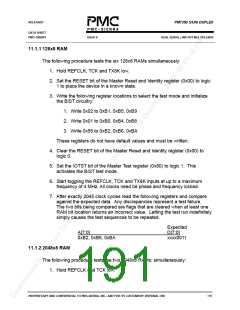
2. Set the RESET bit of the Master Reset and Identity register (0x00) to logic
1 to place the device in a known state.
3. Write the following register locations to select the test mode and initialize
the BIST circuitry:
1. Write 0x02 to 0xDD
2. Write 0x01 to 0xDC
3. Write 0x55 to 0xDE
These registers do not have default values and must be written.
4. Clear the RESET bit of the Master Reset and Identity register (0x00) to
logic 0.
5. Set the IOTST bit of the Master Test register (0x80) to logic 1. This
activates the BIST test mode.
6. Start toggling the REFCLK and TCK inputs at up to a maximum frequency
of 4 MHz. All clocks need be phase and frequency locked.
7. After exactly 32765 clock cycles read the following register and compare
against the expected data. Any discrepancies represent a test failure.
The two bits being compared are flags that are cleared when at least one
RAM bit location returns an incorrect value. Letting the test run indefinitely
simply causes the test sequences to be repeated.
Expected
D[7:0]
xxxx0011
A[7:0]
0xDE
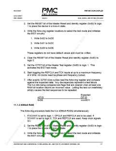
11.1.3 4096x8 RAM
The following procedure tests the two 4096x8 RAMs simultaneously:
1. If SCIANY is set to logic 1, OFCLK and REFCLK are to be used. If
SCIANY is set to logic 0, TCK and REFCLK are used. Keep clock signals
low.
2. Set the RESET bit of the Master Reset and Identity register (0x00) to logic
1 to place the device in a known state.
3. Write the following register locations to select the test mode and initialize
the BIST circuitry:
PROPRIETARY AND CONFIDENTIAL TO PMC-SIERRA, INC., AND FOR ITS CUSTOMERS’ INTERNAL USE
177

 PMC [ PMC-SIERRA, INC ]