RELEASED
PM7350 S/UNI DUPLEX
DATA SHEET
PMC-1980581
ISSUE 8
DUAL SERIAL LINK PHY MULTIPLEXER
11
TEST FEATURES DESCRIPTION
Simultaneously asserting (low) the CSB, RDB and WRB inputs causes all digital
output pins and the data bus to be held in a high-impedance state. This test
feature may be used for board testing.
Test mode registers are used to apply test vectors during production testing of
the S/UNI-DUPLEX. Test mode registers (as opposed to normal mode registers)
are selected when TRS (A[7]) is high.
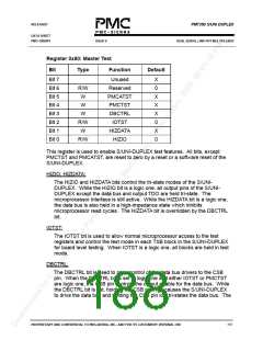
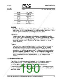
The S/UNI-DUPLEX supports a standard IEEE 1149.1 five-signal JTAG boundary
scan test port for use in board testing. All digital device inputs may be read and
all digital device outputs may be forced with the exception of the RXD1+/-,
RXD2+/-, TXD1+/- and TXD2+/- pins via the JTAG test port.
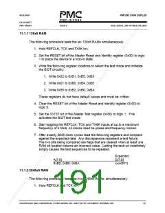
A limited RAM built-in-self-test (BIST) is available.
Notes on Test Mode Register Bits:
1. Writing values into unused register bits has no effect. However, to ensure
software compatibility with future, feature-enhanced versions of the product,
unused register bits must be written with logic zero. Reading back unused bits
can produce either a logic one or a logic zero; hence, unused register bits should
be masked off by software when read.
2. Writable test mode register bits are not initialized upon reset unless otherwise
noted.
PROPRIETARY AND CONFIDENTIAL TO PMC-SIERRA, INC., AND FOR ITS CUSTOMERS’ INTERNAL USE
172

 PMC [ PMC-SIERRA, INC ]