RELEASED
PM7350 S/UNI DUPLEX
DATA SHEET
PMC-1980581
ISSUE 8
DUAL SERIAL LINK PHY MULTIPLEXER
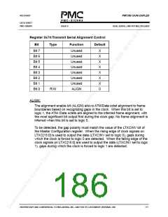
Register 0x74:Transmit Serial Alignment Control
Bit
Type
Function
Default
Bit 7
Bit 6
Bit 5
Bit 4
Bit 3
Bit 2
Bit 1
Bit 0
Unused
Unused
Unused
Unused
Unused
Unused
Unused
ALIGN
X
X
X
X
X
X
X
0
R/W
ALIGN:
The alignment enable bit (ALIGN) allows ATM/Data octet alignment to frame
boundaries based on recognizing gaps in the clock. When this bit is set to
logic 1, the ATM /Data octets are aligned to the inferred frame alignment, with
the most significant bit output first during the clock gap. No frame alignment is
inferred when this bit is set to logic 0.
To be detected, the gap polarity must match the value of the LTXCINV bit of
the Master Configuration register. When the rising edge of clock signals on
LTXC[15:0] is used to output the data (LTXCINV set to logic 0), gaps during
which the clock is forced to logic 0 are detected. When the falling edge of the
clock signals on LTXC[15:0] are used to output the data (LTXCINV set to logic
1), gaps during which the clock is forced to logic 1 are detected.
PROPRIETARY AND CONFIDENTIAL TO PMC-SIERRA, INC., AND FOR ITS CUSTOMERS’ INTERNAL USE
171

 PMC [ PMC-SIERRA, INC ]