S/UNI-IMA-4 Telecom Standard Product Data Sheet
Released
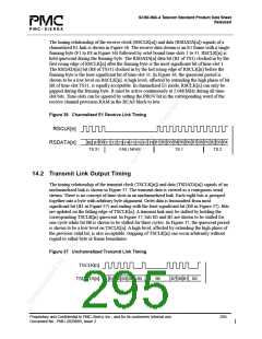
Figure 40 Channelized E1 Transmit Link Timing w/ Clock gapped Low
TSCLK[n]
B8
B2 B3 B4 B5 B6 B7 B8 B1 B2 B3 B4
TS 1 TS 2
B6 B7
TS 31
B1
TSDATA[n]
FAS / NFAS
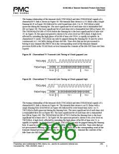
Figure 41 Channelized E1 Transmit Link Timing w/ Clock gapped High
TSCLK[n]
B2 B3 B4 B5 B6 B7 B8 B1 B2 B3 B4
B1
B6 B7 B8
TS 31
TSDATA[n]
FAS / NFAS
TS 1
TS 2
Alternatively, the CTSCLK can be used instead of the TSCLK[n] to lock the clocks of all the
links together
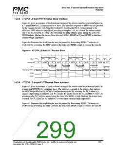
14.3 Any-PHY/UTOPIA L2 Interfaces
While the following diagrams present representative waveforms, they are not an attempt to
unambiguously describe the interfaces. The Pin Description section is intended to present the
detailed pin behavior and constraints on use.
The following parameters apply to all Any-PHY/UTOPIA interface figures:
m = 7 for 8-bit mode, 15 for 16-bit mode
k = is a function of 8/16 bit mode and number of prepends selected.
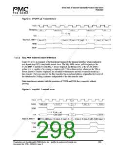
14.3.1 UTOPIA L2 Transmit Slave Interface
Figure 42 gives an example of the functional timing of the transmit interface when configured
as a 31-port UTOPIA L2 compliant transmit slave. The interface responds to the enabled
addresses as defined by the register Transmit Cell Available Enable by asserting the TCA
corresponding to the addressed PHY when it is capable of accepting a complete cell. As a result,
the master selects one of the S/UNI-IMA-4’s PHY’s by presenting the PHY address again
during the last cycle TENB is high. If the device had not been selected, TSOC, TDAT[m:0], and
TPRTY would have remained high-impedance.
Figure 42 illustrates that a cell transfer may be paused by deasserting TENB. The device is
reselected by presenting the PHY’s address the last cycle TENB is high to resume the transfer.
Proprietary and Confidential to PMC-Sierra, Inc., and for its customers’ internal use.
Document No.: PMC-2020889, Issue 2
297

 PMC [ PMC-SIERRA, INC ]