S/UNI-IMA-4 Telecom Standard Product Data Sheet
Released
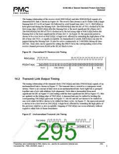
The timing relationship of the receive clock (RSCLK[n]) and data (RSDATA[n]) signals of a
channelized E1 link is shown in Figure 36. The receive data stream is an E1 frame with a single
framing byte (F1 to F8 in Figure 36) followed by octet bound time-slots 1 to 31. RSCLK[n] is
held quiescent during the framing byte. The RSDATA[n] data bit (B1 of TS1) clocked in by the
first rising edge of RSCLK[n] after the framing byte is the most significant bit of time-slot 1.
The RSDATA[n] bit (B8 of TS31) clocked in by the last rising edge of RSCLK[n] before the
framing byte is the least significant bit of time-slot 31. In Figure 36, the quiescent period is
shown to be a low level on RSCLK[n]. A high level, affected by extending the high phase of bit
B8 of time-slot TS31, is equally acceptable. In channelized E1 mode, RSCLK[n] can only be
gapped during the framing byte. It must be active continuously at 2.048 MHz during all time-
slot bits. Time-slots can be ignored by setting the PROV bit in the corresponding word of the
receive channel provision RAM in the RCAS block to low.
Figure 36 Channelized E1 Receive Link Timing
RSCLK[n]
B8
B1 B2 B3 B4 B5 B6 B7 B8 B1 B2 B3 B4
B6 B7
TS 31
F1 F2 F3 F4 F5 F6 F7 F8
FAS / NFAS
RSDATA[n]
TS 1
TS 2
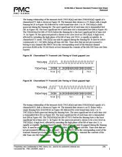
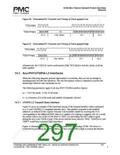
14.2 Transmit Link Output Timing
The timing relationship of the transmit clock (TSCLK[n]) and data (TSDATA[n]) signals of an
unchannelized link is shown in Figure 37. The transmit data is viewed as a contiguous serial
stream. There is no concept of time-slots in an unchannelized link. Each eight bits is grouped
together into a byte with arbitrary byte alignment. Octet data is transmitted from most
significant bit (B1 in Figure 37) and ending with the least significant bit (B8 in Figure 37). Bits
are updated on the falling edge of TSCLK[n]. A transmit link may be stalled by holding the
corresponding TSCLK[n] quiescent. In Figure 37, bits B5 and B2 are shown to be stalled for
one cycle while bit B6 is shown to be stalled for three cycles. In Figure 37, the quiescent period
is shown to be a low level on TSCLK[n]. A high level, affected by extending the high phase of
the previous valid bit, is also acceptable. Gapping of TSCLK[n] can occur arbitrarily without
regard to either byte or frame boundaries.
Figure 37 Unchannelized Transmit Link Timing
TSCLK[n]
B1 B2 B3 B4 B5
B6
B7 B8 B1 B2
TSDATA[n]
Proprietary and Confidential to PMC-Sierra, Inc., and for its customers’ internal use.
Document No.: PMC-2020889, Issue 2
295

 PMC [ PMC-SIERRA, INC ]