S/UNI-IMA-4 Telecom Standard Product Data Sheet
Released
14.4 SDRAM Interface
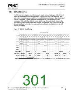
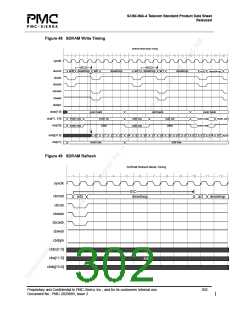
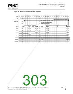
The following three diagrams depict the timing for signals destined for the pins of the SDRAM
during the Activate-Read (with Auto-precharge), Activate-Write (with Auto-precharge), and
Auto-refresh command sequences and Power-Up and Initialization Sequence.. The cbcmd signal
is not an actual signal; it merely represents the memory access command formed by the
combination of the individual SDRAM control signals (e.g., cbcsb and cbrasb). Also note that
reads/writes of cell buffers are always done in bursts of eight words, with 4 bursts per cells; the
first and third bursts involve the even banks and the second and fourth bursts involve the odd
banks in the SDRAM.
Figure 47 SDRAM Read Timing
SDRAM Read Mode Timing
1
2
3
4
5
6
7
8
9
10 11
12
13
14
15 16
17
18
19
20
21 22
23
sysclk
tRCD
act0 desel/nop rd0
tRCD
act desel/nop rd1
tRCD
act2 desel/nop rd2
cbcmd
cbcsb
desel/nop
desel/nop
cbrasb
cbcasb
cbweb
cbdqm
cbbs[1:0]
cba[11, 9:0]
cba[10]
even bank
odd bank
even bank
even row
even row
even co
prea
odd row
odd row
odd col
prea
even row
odd row
even col
prea
cbdq[15:0]
d0
d1
d2
d3 d4
d5
d6
d7
d8 d9 d10 d11 d12 d13 d14 d15
d16
Proprietary and Confidential to PMC-Sierra, Inc., and for its customers’ internal use.
Document No.: PMC-2020889, Issue 2
301

 PMC [ PMC-SIERRA, INC ]