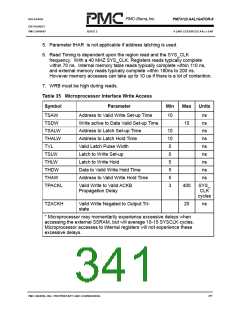
RELEASED
PM73123 AAL1GATOR-8
DATASHEET
PMC-2000097
ISSUE 2
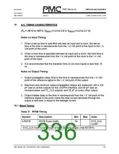
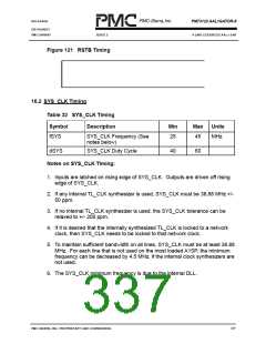
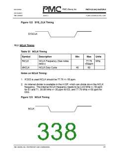
8 LINK CES/DBCES AAL1 SAR
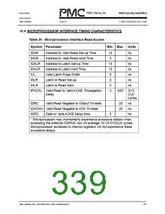
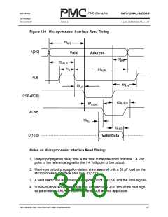
Figure 124 Microprocessor Interface Read Timing
tS
AR
A[9:0]
Valid
Address
tH
AR
tS
ALR
tV
tH
L
ALR
ALE
tH
LR
tS
LR
(CSB+RDB)
ACKB
tZ
ACKH
tP
ACKL
tS
RD
tZ
RD
D[15:0]
Valid Data
Notes on Microprocessor Interface Read Timing:
1. Output propagation delay time is the time in nanoseconds from the 1.4 Volt
point of the reference signal to the 1.4 Volt point of the output.
2. Maximum output propagation delays are measured with a 50 pF load on the
Microprocessor Interface data bus, (D[15:0]).
3. A valid read cycle is defined as a logical OR of the CSB and the RDB signals.
4. In non-multiplexed address/data bus architectures, ALE should be held high
so parameters tSALR, tHALR, tVL, and tSLR are not applicable.
PMC-SIERRA, INC. PROPRIETARY AND CONFIDENTIAL
340

 PMC [ PMC-SIERRA, INC ]