RELEASED
PM73123 AAL1GATOR-8
DATASHEET
PMC-2000097
ISSUE 2
8 LINK CES/DBCES AAL1 SAR
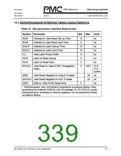
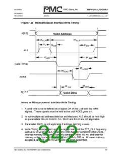
Figure 125 Microprocessor Interface Write Timing
A[9:0]
Valid Address
tS
tH
ALW
ALW
tV
L
tS
tH
LW
LW
ALE
tS
tH
AW
AW
(CSB+WRB)
ACKB
tZ
ACKH
tP
ACKL
tH
tS
DW
DW
D[15:0
Valid Data
Notes on Microprocessor Interface Write Timing:
1. A valid write cycle is defined as a logical OR of the CSB and the WRB
signals. These signals must be held active until ACKB goes low.
2. In non-multiplexed address/data bus architectures, ALE should be held high
so parameters tSALW, tHALW, tVL, tSLW and tHLW are not applicable.
3. Parameter tHAW is not applicable if address latching is used.
4. Write Timing is dependent upon the region read and the SYS_CLK frequency.
With a 40 MHZ SYS_CLK, Registers writes typically complete within 70 ns.
Internal memory table writes typically complete within 110 ns, and external
memory writes typically complete within 180ns to 200 ns. However memory
accesses can take up to 10 us if there is a lot of contention.
PMC-SIERRA, INC. PROPRIETARY AND CONFIDENTIAL
342

 PMC [ PMC-SIERRA, INC ]