PM6341 E1XC
DATA SHEET
PMC-910419
ISSUE 8
E1 FRAMER/TRANSCEIVER
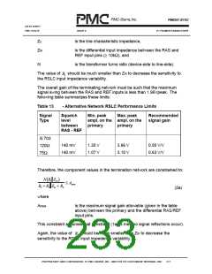
recommended that a transformer have a turns ratio of no more than 1:2. It is also
recommended that the codes presented here be used as a guideline and that the
actual code values be verified (and modified) on the bench with the device
driving the actual transformer and termination expected in the application.
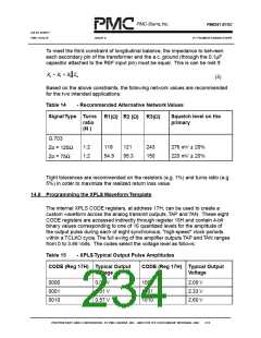
14.9 CODE Register Programming Sequence for Custom Waveforms
To program the XPLS CODE registers for a custom waveform template, the
following sequence should be used:
1. Set the RPT bit in the XPLS Configuration Register to logic 0.
2. Write the CODE register address (0-7) in the XPLS CODE Indirect Address
register.
3. Write the desired code value to the XPLS CODE Indirect Data Register
(register 17H).
4. Repeat steps 2 and 3 until all 8 CODE registers are written.
5. Enable XPLS to generate the new waveform by setting RPT to logic 1.
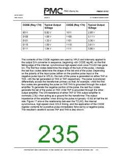
The contents of the XPLS CODE registers can be reviewed at any time by using
the following sequence:
1. Write the CODE register address (0-7) in the XPLS CODE Indirect Address
register.
2. Read the XPLS CODE Indirect Data Register (register 17H).This returns the
code contents of the desired code register.
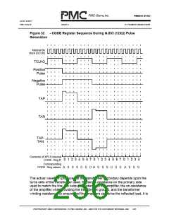
14.10 Using the Digital Jitter Attenuator
The key to using DJAT lies in selecting the appropriate divisors for the phase
comparison between the selected reference clock and the generated smooth
TCLKO.
14.10.1
Default Application
Upon reset, the E1XC default condition provides jitter attenuation with TCLKO
referenced to the transmit clock, BTCLK. The DJAT SYNC bit is also logic 1 by
default. DJAT is configured to divide its input clock rate, BTCLK, and its output
clock rate, TCLKO, both by 48, which is the maximum length of the FIFO. These
divided down clock rates are then used by the phase comparator to update the
PROPRIETARY AND CONFIDENTIAL TO PMC-SIERRA, INC., AND FOR ITS CUSTOMERS’ INTERNAL USE
221

 PMC [ PMC-SIERRA, INC ]