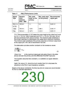
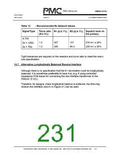
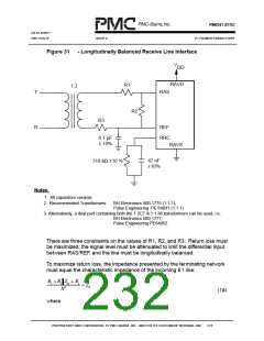
PM6341 E1XC
DATA SHEET
PMC-910419
ISSUE 8
E1 FRAMER/TRANSCEIVER
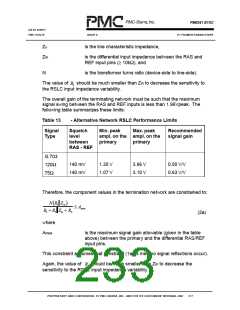
To meet the third constraint of longitudinal balance, the impedance to between
each secondary pin of the transformer and the a.c. ground (through the 0.1µF
capacitor attached to the REF input pin) must be equal. This is can be met if:
=
+
R Z
2
R
R
3
1
in
(3)
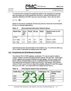
Based on the above constraints, the following network values are recommended
for the two intended applications:
Table 14
- Recommended Alternative Network Values
SignalType Turns
Squelch level on the
primary
R1(Ω) R2 (Ω) R3(Ω)
ratio
(N )
G.703
1:2
1:2
118
121
243
150
276 mV ± 20%
220 mV ± 20%
Zo = 120Ω
Zo = 75Ω
54.9
95.3
Tight tolerances are recommended on the resistors (e.g. 1%) and turns ratio (e.g.
5%) in order to maximize the realized return loss value.
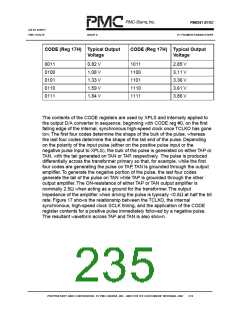
14.8 Programming the XPLS WaveformTemplate
The internal XPLS CODE registers, at address 17H, can be used to create a
custom waveform across the analog transmit outputs, TAP and TAN. These eight
CODE registers are accessed indirectly through register 16H and contain 4-bit
binary values corresponding to one of 16 quantized levels for the amplitude of
the output pulse during each of eight synchronous, "high-speed" clock periods
within a TCLKO cycle. The full swing of the amplifier outputs TAP and TAN ranges
from 0 to 3.86 Volts. The codes select the voltage level as follows:
Table 15
- XPLSTypical Output Pulse Amplitudes
CODE (Reg 17H) Typical Output
Voltage
CODE (Reg 17H) Typical Output
Voltage
0000
0001
0010
0.00 V
0.31 V
0.57 V
1000
1001
1010
2.09 V
2.33 V
2.60 V
PROPRIETARY AND CONFIDENTIAL TO PMC-SIERRA, INC., AND FOR ITS CUSTOMERS’ INTERNAL USE
218

 PMC [ PMC-SIERRA, INC ]