PEX 8532 Transparent Mode Port Registers
PLX Technology, Inc.
11.4.3
PLX-Specific Memory-Mapped Configuration Mechanism
The PLX-Specific Memory-Mapped Configuration mechanism provides a method to access
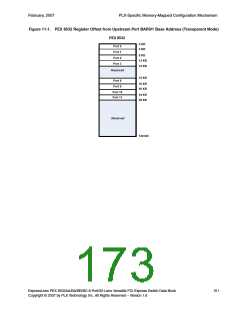
the Configuration registers of each port in a single Memory map, as illustrated in Figure 11-1. The
registers of all ports are contained within a 4-KB range. The PEX 8532 supports up to
eight simultaneously active ports.
The PEX 8532 requires a single contiguous Memory space of 128 KB to contain all the PEX 8532
Configuration registers and sufficient Memory space to support software compatibility for future
device expansion.
To use the PLX-Specific Memory-Mapped Configuration mechanism, program the upstream port’s
Type 1 Configuration Space Base Address 0 and Base Address 1 registers (BAR0 and BAR1,
offsets 10h and 14h, respectively) registers. After the PEX 8532 upstream port Memory-Mapped
register Base Address registers are configured, Port 0 registers can be accessed with Memory Reads
from and Writes to the first 4 KB (0h to FFFh), Port 1 registers can be accessed with Memory Reads
from and Writes to the second 4 KB (1000h to 1FFFh), Port 8 registers can be accessed with Memory
Reads from and Writes to the ninth 4 KB (8000h to 8FFFh), and so forth. Within each of these
4-KB windows, individual registers are located at the DWord offsets indicated in Table 11-1.
The upstream port BAR0 and BAR1 registers are typically enumerated at boot time, by BIOS or
the Operating System (OS) software. When the registers are written (by serial EEPROM or software),
the PEX 8532 automatically copies the values into the BAR0 and BAR1 Shadow registers that exist in
Ports 0 and 8, located at offsets 6C0h through 71Ch. The particular registers used within this block
depend upon which port is the upstream port.
If the upstream port BAR0 and BAR1 registers are enumerated by serial EEPROM, rather than by
BIOS/OS, the serial EEPROM must be programmed to also load the same values to the corresponding
BAR0 and BAR1 Shadow registers in each station.
Note: The shadow registers provide for another option. After BAR0 and BAR1 are programmed, it is
possible to overwrite the “shadowed” location (using the serial EEPROM or software) to set up
non-tree hierarchies, in which each station can have different Memory windows. If doing this,
it is recommended to match the upstream station shadow register with the BARs.
150
ExpressLane PEX 8532AA/BA/BB/BC 8-Port/32-Lane Versatile PCI Express Switch Data Book
Copyright © 2007 by PLX Technology, Inc. All Rights Reserved – Version 1.6

 PLX [ PLX TECHNOLOGY ]