Philips Semiconductors
Objective specification
Integrated PAL and PAL/NTSC TV
processors
TDA8360; TDA8361; TDA8362
To overcome this problem a speed-up
circuit has been included which
detects whether the AGC detector is
activated every frame period. If,
during a 3-frame period, no action is
detected the speed of the system is
increased. When the incoming signal
has no peak white information (e.g.
test lines in the vertical retrace period)
the gain would be video signal
dependent. To avoid this effect the
circuit also contains a black level
AGC detector which is activated when
the black level of the video signal
exceeds a certain level.
SYMBOL
VFB
PIN
DESCRIPTION
vertical feedback input
41
42
43
44
45
46
47
48
49
50
51
52
VRAMP
VOUT
vertical ramp generator
vertical output
AFCOUT
IFIN1
AFC output
IF input 1
IFIN2
IF input 2
AGCOUT
DECAGC
TUNEADJ
AUOUT
DECDEM
DECBG
tuner AGC output
AGC decoupling capacitor
tuner take-over adjustment
audio output
decoupling sound demodulator
decoupling bandgap supply
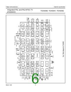
The TDA8361 and TDA8362 contain
a video identification circuit which is
independent of the synchronization
circuit. Therefore search tuning is
possible when the display section of
the receiver is used as a monitor. In
the TDA8360 this circuit is only used
for stable OSD at no signal input. In
the normal television mode the
The reference carrier for the video
TDA8360
demodulator is obtained by means of
passive regeneration of the picture
carrier. The external reference tuned
circuit is the only remaining
The TDA8360 has the following
differences to the pinning:
Pin 6: external audio input not
connected
adjustment of the IC.
In the TDA8362 the polarity of the
demodulator can be switched so that
the circuit is suitable for both positive
and negative modulated signals.
identification output is connected to
the coincidence detector, this applies
to all three devices. The identification
output voltage is LOW when no
transmitter is identified. In this
Pin 15: external CVBS input not
connected
Pin 16: chrominance and A/V switch
input not connected
The AFC circuit is driven with the
same reference signal as the video
demodulator. To ensure that the
video content does not disturb the
AFC operation a sample-and-hold
circuit is incorporated; the capacitor
for this function is internal. The AFC
output voltage is 6 V.
condition the sound demodulator is
switched off (mute function). When a
transmitter is identified the output
voltage is HIGH. The voltage level is
dependent on the frequency of the
incoming chrominance signal.
Pin 27: hue control input not
connected.
TDA8361
The TDA8361 has the following
differences to the pinning:
Pin 1: only audio de-emphasis
Pin 27: only hue control
The AGC detector operates on levels,
top sync for negative modulated and
top white for positive modulated
signals.The AGC detector time
constant capacitor is connected
externally. This is mainly because of
the flexibility of the application.
Pin 32: 4.43 MHz output for TDA8395
is not connected.
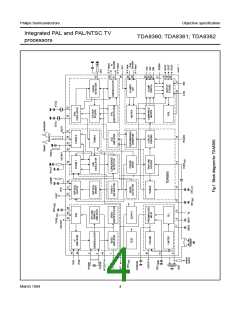
FUNCTIONAL DESCRIPTION
Video IF amplifier
The time constant of the AGC system
during positive modulation
The IF amplifier contains
(TDA8362) is slow, this is to avoid any
visible picture variations. This,
however, causes the system to react
very slowly to sudden changes in the
input signal amplitude.
3 AC-coupled control stages with a
total gain control range of greater
than 60 dB. The sensitivity of the
circuit is comparable with that of
modern IF ICs.
March 1994
8

 NXP [ NXP ]