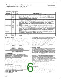
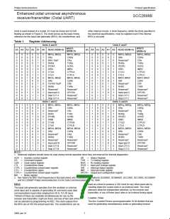
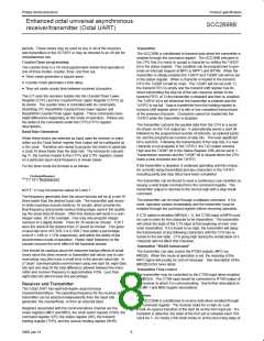
Philips Semiconductors
Product specification
Enhanced octal universal asynchronous
receiver/transmitter (Octal UART)
SCC2698B
Note: The transmitter may also control the “RTSN” pin. When un-
der transmitter control the meaning is completely changed. The
meaning is the transmission has ended. This signal is usually used
to switch (turnaround) a bi–directional driver from transmit to re-
ceive.
the receiver, thereby withdrawing its interrupt. If, at this time, the
interrupt service begins for the previously seen interrupt, a read of
the ISR will show the “Counter Ready” bit not set. If nothing else is
interrupting, this read of the ISR will return a x’00 character.
Receiver Reset and Disable
If the receiver is disabled, the FIFO characters can be read. Howev-
er, no additional characters can be received until the receiver is
enabled again. If the receiver is reset, the FIFO and all of the re-
ceiver status, and the corresponding output ports and interrupt are
reset. No additional characters can be received until the receiver is
enabled again.
Receiver disable stops the receiver immediately – data being
assembled if the receiver shift register is lost. Data and status in the
FIFO is preserved and may be read. A re-enable of the receiver
after a disable will cause the receiver to begin assembling
characters at the next start bit detected. A receiver reset will discard
the present shift register data, reset the receiver ready bit (RxRDY),
clear the status of the byte at the top of the FIFO and re-align the
FIFO read/write pointers. This has the appearance of “clearing or
flushing” the receiver FIFO. In fact, the FIFO is NEVER cleared!
The data in the FIFO remains valid until overwritten by another
received character. Because of this, erroneous reading or extra
reads of the receiver FIFO will miss-align the FIFO pointers and
result in the reading of previously read data. A receiver reset will
re-align the pointers.
Receiver Time–out Mode
The time–out mode uses the received data stream to control the
counter. Each time a received character is transferred from the shift
register to the RxFIFO, the counter is restarted. If a new character
is not received before the counter reaches zero count, the counter
ready bit is set, and an interrupt can be generated. This mode can
be used to indicate when data has been left in the RxFIFO for more
than the programmed time limit. Otherwise, if the receiver has been
programmed to interrupt the CPU when the receive FIFO is full, and
the message ends before the FIFO is full, the CPU may not know
there is data left in the FIFO. The CTPU and CTPL value would be
programmed for just over one character time, so that the CPU would
be interrupted as soon as it has stopped receiving continuous data.
This mode can also be used to indicate when the serial line has
been marking for longer than the programmed time limit. In this
case, the CPU has read all of the characters from the FIFO, but the
last character received has started the count. If there is no new
data during the programmed time interval, the counter ready bit will
get set, and an interrupt can be generated.
WAKE-UP MODE
In addition to the normal transmitter and receiver operation
described above, the Octal UART incorporates a special mode
which provides automatic wake-up of the receiver through address
frame recognition for multiprocessor communications. This mode is
selected by programming bits MR1[4:3] to ‘11’.
In this mode of operation, a ‘master’ station transmits an address
character followed by data characters for the addressed ‘slave’
station. The slave stations, whose receivers are normally disabled,
examine the received data stream and ‘wake-up’ the CPU [by
setting RxRDY) only upon receipt of an address character. The CPU
compares the received address to its station address and enables
the receiver if it wishes to receive the subsequent data characters.
Upon receipt of another address character, the CPU may disable the
receiver to initiate the process again.
The time–out mode is enabled by writing the appropriate command
to the command register. Writing an ‘Ax’ to CRA or CRB will invoke
the time–out mode for that channel. Writing a ‘Cx’ to CRA or CRB
will disable the time–out mode. The time–out mode should only be
used by one channel at once, since it uses the C/T. If, however, the
time–out mode is enabled from both receivers, the time–out will
occur only when both receivers have stopped receiving data for the
time–out period. CTPU and CTPL must be loaded with a value
greater than the normal receive character period. The time–out
mode disables the regular START/STOP Counter commands and
puts the ca/T into counter mode under the control of the received
data stream. Each time a received character is transferred from the
shift register to the RxFIFO, the C/T is stopped after 1 C/T clock,
reloaded with the value in CTPU and CTPL and then restarted on
the next C/T clock. If the C/T is allowed to end the count before a
new character has been received, the counter ready bit, ISR[3], will
be set. If IMR[3] is set, this will generate an interrupt. Receiving a
character after the C/T has timed out will clear the counter ready bit,
ISR[3], and the interrupt. Invoking the ‘Set Time–out Mode On’
command, CRx = ‘Ax’, will also clear the counter ready bit and stop
the counter until the next character is received.
A transmitted character consists of a start bit, the programmed
number of data bits, an address/data (A/D) bit, and the programmed
number of stop bits. The polarity of the transmitted A/D bit is
selected by the CPU by programming bit MR1[2]; MR1[2] = 0
transmits a zero in the A/D bit position which identifies the
corresponding data bits as data; MR1[2] = 1 transmits a one in the
A/D bit position which identifies the corresponding data bits as an
address. The CPU should program the mode register prior to
loading the corresponding data bits in the THR.
While in this mode, the receiver continuously looks at the received
data stream, whether it is enabled or disabled. If disabled, it sets the
RxRDY status bit and loads the character in the RHR FIFO if the
received A/D bit is a one, but discards the received character if the
received A/D bit is a zero. If enabled, all received characters are
then transferred to the CPU via the RHR. In either case, the data
bits are loaded in the data FIFO while the A/D bit is loaded in the
status FIFO position normally used for parity error (SR[5]). Framing
error, overrun error, and break detect operate normally whether or
not the receiver is enabled.
This mode is cleared by issuing the “Disable Time–out Mode” com-
mand (C0) in the command register.
Time Out Mode Caution
When operating in the special time out mode, it is possible to gener-
ate what appears to be a “false interrupt” – an interrupt without a
cause. This may result when a time–out interrupt occurs and then,
BEFORE the interrupt is serviced, another character is received,
i.e., the data stream has started again. (The interrupt latency is
longer than the pause in the data stream.) In this case, when a new
character has been receiver, the counter/timer will be restarted by
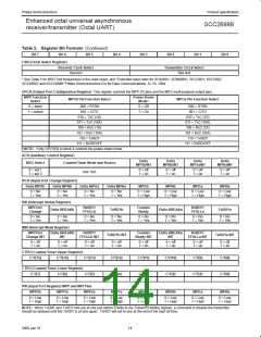
The CTS, RTS, CTS Enable Tx signals
CTS (Clear To Send) is usually meant to be a signal to the transmit-
ter meaning that it may transmit data to the receiver. The CTS input
is on pin MPI0 for the transmitter. The CTS signal is active low;
thus, it is called CTSN. RTS is usually meant to be a signal from the
10
2000 Jan 31

 NXP [ NXP ]