Philips Semiconductors
Product specification
Enhanced octal universal asynchronous
receiver/transmitter (Octal UART)
SCC2698B
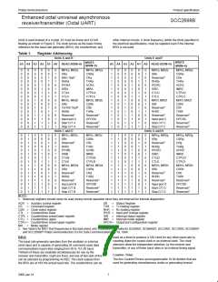
PIN DESCRIPTION (Continued)
PIN
NO.
MNEMONIC
TYPE
NAME AND FUNCTION
MPI1a–MPI1h
14, 21,
38, 40,
60, 62,
78, 80
I
Multi-Purpose Input 1: This pin (one for each UART) is programmable. Its state can always be
determined by reading the IPCR bit 1 or IPR bit 1.
C/TCLK – This input will serve as the external clock for the counter/timer when ACR[5] is set to 0.
This occurs only for channels a, c, e, and g since there is one counter/timer for each DUART block.
This pin is provided with a change-of-state detector.
MPP1a–MPP1h 24, 26,
I/O
I/O
I
Multi-Purpose Pin 1: This pin (one for each UART) is programmed to be an input or an output
according to the state of OPCR[7]. (0 = input, 1 = output). The state of the multi-purpose pin can
always be determined by reading the IPR. When programmed as an input, it will be the transmitter
clock (TxCLK). It will be 1x or 16x according to the clock select registers (CSR[3.0]). When
programmed as an output, it will be the status register TxRDY bit. These pins have a small pull-up
device.
42, 44,
64, 66,
82, 84
MPP2a–MPP2h 28, 30,
Multi-Purpose Pin 2: This pin (one for each UART) is programmed to be an input or an output
according to the state of OPCR[7]. (0 = input, 1 = output). The state of the multi-purpose pin can
always be determined by reading the IPR. When programmed as an input, it will be the receiver clock
(RxCLK). It will be 1x or 16x according to the clock select registers (CSR[7:4). When programmed as
an output, it will be the ISR status register RxRDY/FIFO full bit. These pins have a small pull-up
device.
48, 50,
68, 70,
2, 4
Test Input
–
Test Input: This pin is used as an input for test purposes at the factory while in test mode. This pin
can be treated as ‘N/C’ by the user. It can be tied high, or left open.
V
5, 45
I
I
Power Supply: +5V supply input.
CC
GND
20, 65
Ground
Associated with the interrupt system are the interrupt mask register
BLOCK DIAGRAM
(IMR) and the interrupt status register (ISR). The IMR can be
programmed to select only certain conditions, of the above, to cause
INTRN to be asserted. The ISR can be read by the CPU to
determine all currently active interrupting conditions. However, the
bits of the ISR are not masked by the IMR. The transmitter ready
status and the receiver ready or FIFO full status can be provided on
MPP1a, MPP1b, MPP2a, and MPP2b by setting OPCR[7]. these
outputs are not masked by IMR.
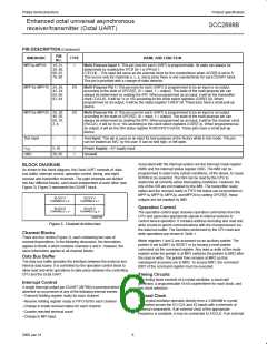
As shown in the block diagram, the Octal UART consists of: data
bus buffer, interrupt control, operation control, timing, and eight
receiver and transmitter channels. The eight channels are divided
into four different blocks, each block independent of each other (see
Figure 3). Figure 2 represents the DUART block.
BLOCK A
BLOCK C
CHANNELS e, f
CHANNELS a, b
Operation Control
BLOCK B
CHANNELS c, d
BLOCK D
CHANNELS g, h
The operation control logic receives operation commands from the
CPU and generates appropriate signals to internal sections to
control device operation. It contains address decoding and read and
write circuits to permit communications with the microprocessor via
the data bus buffer. The functions performed by the CPU read and
write operations are shown in Table 1.
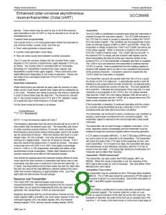
SD00186
Figure 3. Channel Architecture
Channel Blocks
There are four blocks (Figure 3), each containing two sets of
receiver/transmitters. In the following discussion, the description
applies to Block A which contains channels a and b. However, the
same information applies to all channel blocks.
Mode registers 1 and 2 are accessed via an auxiliary pointer. The
pointer is set to MR1 by RESET or by issuing a reset pointer
command via the command register. Any read or write of the mode
register while the pointer is at MR1 switches the pointer to MR2 after
the read or write. The pointer then remains at MR2 so that
subsequent accesses are to MR2. To access MR1, the command
0001 of the command register must be executed.
Data Bus Buffer
The data bus buffer provides the interface between the external and
internal data buses. It is controlled by the operation control block to
allow read and write operations to take place between the controlling
CPU and the Octal UART.
Timing Circuits
The timing block consists of a crystal oscillator, a baud rate
generator, a programmable 16-bit counter/timer for each block, and
two clock selectors.
Interrupt Control
A single interrupt output per DUART (INTRN) is provided which is
asserted on occurrence of any of the following internal events:
–Transmit holding register ready for each channel
Crystal Clock
The crystal oscillator operates directly from a 3.6864MHz crystal
connected across the X1/ CLK and X2 inputs with a minimum of
external components. If an external clock of the appropriate
frequency is available, it may be connected to X1/CLK. If an external
–Receive holding register ready or FIFO full for each channel
–Change in break received status for each channel
–Counter reached terminal count
–Change in MPI input
6
2000 Jan 31

 NXP [ NXP ]