Philips Semiconductors
Product specification
Dual asynchronous receiver/transmitter (DUART)
SCC2692
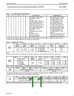
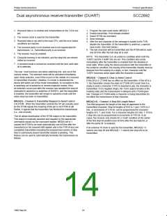
Table 2. Register Bit Formats (Continued)
BIT 7
BIT 6
BIT 5
BIT 4
BIT 3
BIT 2
BIT 1
BIT 0
RECEIVED
BREAK*
FRAMING
ERROR*
PARITY
ERROR*
OVERRUN
ERROR
SRA
SRB
TxEMT
TxRDY
FFULL
RxRDY
0 = No
0 = No
0 = No
0 = No
0 = No
0 = No
0 = No
0 = No
1 = Yes
1 = Yes
1 = Yes
1 = Yes
1 = Yes
1 = Yes
1 = Yes
1 = Yes
NOTE: *These status bits are appended to the corresponding data character in the receive FIFO. A read of the status provides these bits
(7:5) from the top of the FIFO together with bits (4:0). These bits are cleared by a “reset error status” command. In character mode they are
discarded when the corresponding data character is read from the FIFO. In block error mode, block error conditions must be cleared by using
the error reset command (command 4x) or a receiver reset.
BIT 7
OP7
BIT 6
OP6
BIT 5
OP5
BIT 4
OP4
BIT 3
BIT 2
BIT 1
BIT 0
OP3
00 = OPR[3]
01 = C/T OUTPUT
10 = TxCB(1X)
11 = RxCB(1X)
OP2
0 = OPR[7]
1 = TxRDYB 1 = TxRDYA 1 = RxRDY/
FFULLB
0 = OPR[6]
0 = OPR[5]
0 = OPR[4]
1 = RxRDY/
FFULLA
00 = OPR[2]
OPCR
01 = TxCA(16X)
10 = TxCA(1X)
11 = RxCA(1X)
OPR
BIT 7
BIT 6
BIT 5
BIT 4
BIT 3
BIT 2
BIT 1
BIT 0
OPR bit
OP pin
0
1
1
0
0
1
1
0
0
1
1
0
0
1
1
0
0
1
1
0
0
1
1
0
0
1
1
0
0
1
1
0
NOTE:
The level at the OP pin is the inverse of the bit in the OPR register.
BIT 7
BIT 6
BIT 5
BIT 4
BIT 3
BIT 2
BIT 1
BIT 0
BRG SET
SELECT
COUNTER/TIMER
MODE AND SOURCE
DELTA
IP 3 INT
DELTA
IP 2 INT
DELTA
IP 1 INT
DELTA
IP 0 INT
ACR
0 = set 1
1 = set 2
0 = Off
1 = On
0 = Off
1 = On
0 = Off
1 = On
0 = Off
1 = On
See Table 4
BIT 7
BIT 6
BIT 5
BIT 4
BIT 3
IP 3
BIT 2
IP 2
BIT 1
IP 1
BIT 0
IP 0
DELTA
IP 3
DELTA
IP 2
DELTA
IP 1
DELTA
IP 0
IPCR
0 = No
1 = Yes
0 = No
1 = Yes
0 = No
1 = Yes
0 = No
1 = Yes
0 = Low
1 = High
0 = Low
1 = High
0 = Low
1 = High
0 = Low
1 = High
BIT 7
BIT 6
BIT 5
BIT 4
BIT 3
BIT 2
BIT 1
BIT 0
INPUT
PORT
CHANGE
DELTA
BREAK B
RxRDY/
FFULLB
COUNTER
READY
DELTA
BREAK A
RxRDY/
FFULLA
TxRDYB
TxRDYA
ISR
IMR
0 = No
1 = Yes
0 = No
1 = Yes
0 = No
1 = Yes
0 = No
1 = Yes
0 = No
1 = Yes
0 = No
1 = Yes
0 = No
1 = Yes
0 = No
1 = Yes
BIT 7
BIT 6
BIT 5
BIT 4
BIT 3
BIT 2
BIT 1
BIT 0
IN. PORT
CHANGE
INT
DELTA
BREAK B
INT
RxRDY/
FFULLB
INT
COUNTER
READY
INT
DELTA
BREAK A
INT
RxRDY/
FFULLA
INT
TxRDYB
INT
TxRDYA
INT
0 = Off
1 = On
0 = Off
1 = On
0 = Off
1 = On
0 = Off
1 = On
0 = Off
1 = On
0 = Off
1 = On
0 = Off
1 = On
0 = Off
1 = On
BIT 7
BIT 6
BIT 5
BIT 4
BIT 3
BIT 2
BIT 1
BIT 0
CTUR
CTLR
C/T[15]
C/T[14]
C/T[13]
C/T[12]
C/T[11]
C/T[10]
C/T[9]
C/T[8]
BIT 7
BIT 6
BIT 5
BIT 4
BIT 3
BIT 2
BIT 1
BIT 0
C/T[7]
C/T[6]
C/T[5]
C/T[4]
C/T[3]
C/T[2]
C/T[1]
C/T[0]
12
1998 Sep 04

 NXP [ NXP ]