Philips Semiconductors
Product specification
Multimedia bridge, high performance
Scaler and PCI circuit (SPCI)
SAA7146A
address phase
first data phase
write data
second data phase
handbook, full pagewidth
t
t
as
ah
address
write data
AD(WR)
AD(RD)
SBHE
ALE
t
dsw
address
read data
read data
t
dhr
t
dsrd
t
t
t
az
dsrh
dhw
t
RDN
WRN
rwi
RDY
t
t
rdy
min
MHB064
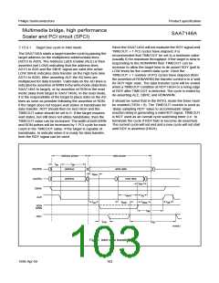
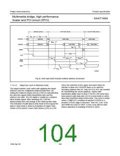
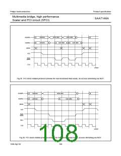
Fig.32 Intel style block transfer without address increment.
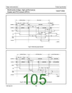
Since the selection of the upper and lower bytes for
transfer is done via LDS/UDS there is no need for
decoding address line A0. Only AD15 to AD1 are needed
for transmitting the (word-)address. Slaves with
handshake ability have to drive DTACK LOW when they
have placed valid data onto AD16 in read mode or when
they have read their data in write mode. The cycle is ended
when a TIMEOUT condition at inactive DTACK or a
positive DTACK edge is detected. Then AS, LDS, UDS
and RWN are reset to HIGH. A new cycle will not start
before detection of resetting DTACK to HIGH.
7.15.4.2 Target bus cycle in Motorola mode
The target transfer cycle starts with applying the target
address onto the multiplexed address/data lines. By
setting the Address Strobe (AS) to LOW it is indicated that
the direction signal RWN (Read/Write Not) and the
address are valid. The AS signal is usable as a address
latch enable signal. After asserting AS LOW the
address/data lines will change to the data transfer state.
The indication of valid data in write mode or the request for
data in read mode is done by transition of Upper Data
Strobe (UDS) and/or Lower Data Strobe (LDS) to LOW.
1998 Apr 09
104

 NXP [ NXP ]