Philips Semiconductors
Product specification
Multimedia bridge, high performance
Scaler and PCI circuit (SPCI)
SAA7146A
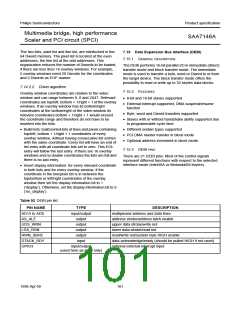
7.15.4 FUNCTIONAL DESCRIPTION
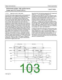
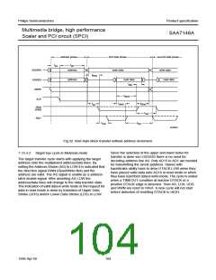
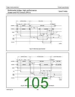
An immediate access cycle consists of one address phase and one data phase. A block transfer with address increment
enabled consists of several consecutive address/data phase couples. A block transfer with disabled address increment
consists of one address phase followed by several data phases. The AS_ALE signal toggles only for a new address
phase.The single bytes or words are assembled/disassembled to/from Dwords. This includes byte lane swapping since
8-bit devices use for data transfer AD7 to AD0 only, (AD15 to AD8 are used in address phase too, since all 16 AD lines
are used for addressing.)
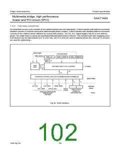
handbook, full pagewidth
block length
command words
DMA address
DEBI_AD
DEBI_CONFIG
DEBI_COMMAND
immed.
data
32
DEBI
FIFO
32
DATA MUX AND CYCLE CONTROL
status
32
32
32
TRANSFER CONTROL AND DATA ASSEMBLING/DISASSEMBLING
8
SAA7146A
8
AS_ALE
LDS_RDN
RWN_SBHE
16/8-bit
slave
UDS_WRN
DTACK_RDY
GPIO3
(XIRQ)
AD16 (15 to 0)
multiplexed
adress/data lines
target bus control signals
Motorola style
MHB062
Intel style
Fig.30 DEBI interface.
1998 Apr 09
102

 NXP [ NXP ]