PCF8574; PCF8574A
NXP Semiconductors
Remote 8-bit I/O expander for I2C-bus with interrupt
7. Functional description
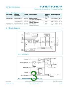
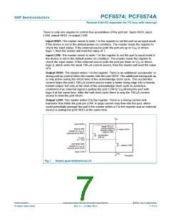
Refer to Figure 1 “Block diagram”.
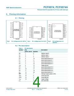
7.1 Device address
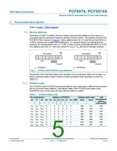
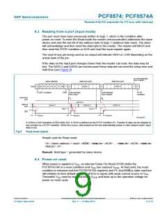
Following a START condition, the bus master must send the address of the slave it is
accessing and the operation it wants to perform (read or write). The address format of the
PCF8574/74A is shown in Figure 6. Slave address pins A2, A1 and A0 are held HIGH or
LOW to choose one of eight slave addresses. To conserve power, no internal pull-up
resistors are incorporated on A2, A1 or A0, so they must be externally held HIGH or LOW.
The address pins (A2, A1, A0) can connect to VDD or VSS directly or through resistors.
R/W
0
R/W
0
slave address
slave address
0
1
0
0
A2 A1 A0
0
1
1
1
A2 A1 A0
fixed
hardware
selectable
fixed
hardware
selectable
002aad628
002aad629
a. PCF8574
Fig 6. PCF8574 and PCF8574A slave addresses
b. PCF8574A
The last bit of the first byte defines the operation to be performed. When set to logic 1 a
read is selected, while a logic 0 selects a write operation (write operation is shown in
Figure 6).
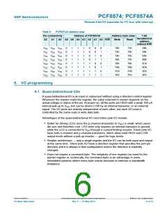
7.1.1 Address maps
The PCF8574 and PCF8574A are functionally the same, but have a different fixed portion
(A6 to A3) of the slave address. This allows eight of the PCF8574 and eight of the
PCF8574A to be on the same I2C-bus without address conflict.
Table 4.
Pin connectivity
A2 A1 A0 A6 A5 A4 A3 A2 A1 A0 R/W
PCF8574 address map
Address of PCF8574
Address byte value
7-bit
hexadecimal
address
Write
Read
without R/W
VSS VSS VSS
VSS VSS VDD
VSS VDD VSS
VSS VDD VDD
VDD VSS VSS
VDD VSS VDD
VDD VDD VSS
VDD VDD VDD
0
0
0
0
0
0
0
0
1
1
1
1
1
1
1
1
0
0
0
0
0
0
0
0
0
0
0
0
0
0
0
0
0
0
0
0
1
1
1
1
0
0
1
1
0
0
1
1
0
1
0
1
0
1
0
1
-
-
-
-
-
-
-
-
40h
42h
44h
46h
48h
4Ah
4Ch
4Eh
41h
43h
45h
47h
49h
4Bh
4Dh
4Fh
20h
21h
22h
23h
24h
25h
26h
27h
PCF8574_PCF8574A
All information provided in this document is subject to legal disclaimers.
© NXP B.V. 2013. All rights reserved.
Product data sheet
Rev. 5 — 27 May 2013
5 of 33

 NXP [ NXP ]