PCF8574; PCF8574A
NXP Semiconductors
Remote 8-bit I/O expander for I2C-bus with interrupt
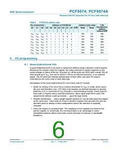
Table 2.
Ordering options …continued
Type number
Orderable
Package Packing method
Minimum Temperature range
part number
order
quantity
PCF8574TS/3 PCF8574TS/3,112 SSOP20 Standard marking
* IC’s tube - DSC bulk pack
1350
2500
2500
Tamb = 40 C to +85 C
Tamb = 40 C to +85 C
PCF8574TS/3,118 SSOP20 Reel 13” Q1/T1
*standard mark SMD
PCF8574ATS/3 PCF8574ATS/3,118 SSOP20 Reel 13” Q1/T1
*standard mark SMD
Tamb = 40 C to +85 C
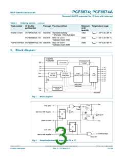
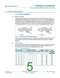
5. Block diagram
PCF8574
PCF8574A
INTERRUPT
LOGIC
LP FILTER
INT
A0
A1
A2
P0
P1
P2
8 bits
SCL
SDA
2
P3
P4
P5
P6
P7
SHIFT
REGISTER
I/O
PORT
INPUT
FILTER
I C-BUS
CONTROL
write pulse
read pulse
POWER-ON
RESET
V
DD
V
SS
002aad624
Fig 1. Block diagram
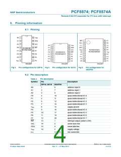
V
DD
I
I
OH
write pulse
100 μA
I
trt(pu)
D
Q
data from Shift Register
FF
P0 to P7
OL
CI
S
power-on reset
V
SS
D
Q
FF
S
CI
read pulse
to interrupt logic
data to Shift Register
002aac109
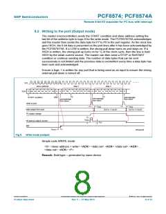
Fig 2. Simplified schematic diagram of P0 to P7
PCF8574_PCF8574A
All information provided in this document is subject to legal disclaimers.
© NXP B.V. 2013. All rights reserved.
Product data sheet
Rev. 5 — 27 May 2013
3 of 33

 NXP [ NXP ]