PCF8574; PCF8574A
NXP Semiconductors
Remote 8-bit I/O expander for I2C-bus with interrupt
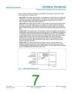
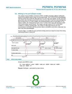
8.2 Writing to the port (Output mode)
The master (microcontroller) sends the START condition and slave address setting the
last bit of the address byte to logic 0 for the write mode. The PCF8574/74A acknowledges
and the master then sends the data byte for P7 to P0 to the port register. As the clock line
goes HIGH, the 8-bit data is presented on the port lines after it has been acknowledged by
the PCF8574/74A. If a LOW is written, the strong pull-down turns on and stays on. If a
HIGH is written, the strong pull-up turns on for 1⁄2 of the clock cycle, then the line is held
HIGH by the weak current source. The master can then send a STOP or ReSTART
condition or continue sending data. The number of data bytes that can be sent
successively is not limited and the previous data is overwritten every time a data byte has
been sent and acknowledged.
Ensure a logic 1 is written for any port that is being used as an input to ensure the strong
external pull-down is turned off.
SCL
1
2
3
4
5
6
7
8
9
slave address
data 1
data 2
SDA
S
A6 A5 A4 A3 A2 A1 A0
0
A
P7 P6
1
P4 P3 P2 P1 P0
A
P7 P6
0
P4 P3 P2 P1 P0
A
P5
P5
START condition
write to port
R/W
acknowledge
from slave
acknowledge
from slave
acknowledge
from slave
t
t
v(Q)
v(Q)
data output from port
P5 output voltage
DATA 1 VALID
DATA 2 VALID
I
trt(pu)
P5 pull-up output current
INT
I
OH
t
d(rst)
002aah349
Fig 8. Write mode (output)
Simple code WRITE mode:
<S> <slave address + write> <ACK> <data out> <ACK> <data out> <ACK> ...
<data out> <ACK> <P>
Remark: Bold type = generated by slave device.
PCF8574_PCF8574A
All information provided in this document is subject to legal disclaimers.
© NXP B.V. 2013. All rights reserved.
Product data sheet
Rev. 5 — 27 May 2013
8 of 33

 NXP [ NXP ]