PCF8574; PCF8574A
NXP Semiconductors
Remote 8-bit I/O expander for I2C-bus with interrupt
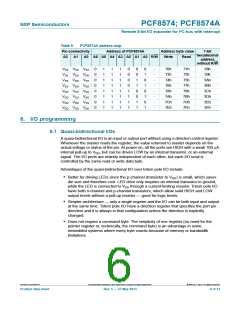
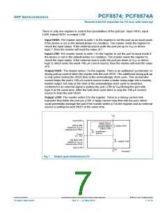
There is only one register to control four possibilities of the port pin: Input HIGH, input
LOW, output HIGH, or output LOW.
Input HIGH: The master needs to write 1 to the register to set the port as an input mode
if the device is not in the default power-on condition. The master reads the register to
check the input status. If the external source pulls the port pin up to VDD or drives
logic 1, then the master will read the value of 1.
Input LOW: The master needs to write 1 to the register to set the port to input mode if
the device is not in the default power-on condition. The master reads the register to
check the input status. If the external source pulls the port pin down to VSS or drives
logic 0, which sinks the weak 100 A current source, then the master will read the value
of 0.
Output HIGH: The master writes 1 to the register. There is an additional ‘accelerator’ or
strong pull-up current when the master sets the port HIGH. The additional strong pull-up
is only active during the HIGH time of the acknowledge clock cycle. This accelerator
current helps the port’s 100 A current source make a faster rising edge into a heavily
loaded output, but only at the start of the acknowledge clock cycle to avoid bus
contention if an external signal is pulling the port LOW to VSS/driving the port with
logic 0 at the same time. After the half clock cycle there is only the 100 A current
source to hold the port HIGH.
Output LOW: The master writes 0 to the register. There is a strong current sink
transistor that holds the port pin LOW. A large current may flow into the port, which
could potentially damage the part if the master writes a 0 to the register and an external
source is pulling the port HIGH at the same time.
V
DD
input HIGH
pull-up with
weak 100 µA
current source
(inactive when
output LOW)
output HIGH
resistor to V
or
DD
external drive HIGH
accelerator
pull-up
P port
P7 - P0
pull-down with
output LOW
resistor to V or
SS
external drive LOW
input LOW
V
SS
002aah683
Fig 7. Simple quasi-bidirectional I/O
PCF8574_PCF8574A
All information provided in this document is subject to legal disclaimers.
© NXP B.V. 2013. All rights reserved.
Product data sheet
Rev. 5 — 27 May 2013
7 of 33

 NXP [ NXP ]