PCF8574; PCF8574A
NXP Semiconductors
Remote 8-bit I/O expander for I2C-bus with interrupt
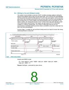
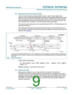
8.3 Reading from a port (Input mode)
The port must have been previously written to logic 1, which is the condition after
power-on reset. To enter the Read mode the master (microcontroller) addresses the slave
device and sets the last bit of the address byte to logic 1 (address byte read). The slave
will acknowledge and then send the data byte to the master. The master will NACK and
then send the STOP condition or ACK and read the input register again.
The read of any pin being used as an output will indicate HIGH or LOW depending on the
actual state of the pin.
If the data on the input port changes faster than the master can read, this data may be
lost. The DATA 2 and DATA3 are lost because these data did not meet the setup time and
hold time (see Figure 9).
no acknowledge
from master
slave address
data from port
DATA 1
data from port
DATA 4
SDA
S
A6 A5 A4 A3 A2 A1 A0
1
A
A
1
P
START condition
R/W acknowledge
from slave
acknowledge
from master
STOP
condition
read from
port
DATA 2
data at
port
DATA 1
DATA 3
DATA 4
t
t
su(D)
h(D)
INT
t
t
t
rst(INT)
v(INT)
rst(INT)
002aah383
A LOW-to-HIGH transition of SDA while SCL is HIGH is defined as the STOP condition (P). Transfer of data can be stopped at
any moment by a STOP condition. When this occurs, data present at the last acknowledge phase is valid (output mode). Input
data is lost.
Fig 9. Read mode (input)
Simple code for Read mode:
<S> <slave address + read> <ACK> <data in> <ACK> ... <data in> <ACK> <data in>
<NACK> <P>
Remark: Bold type = generated by slave device.
8.4 Power-on reset
When power is applied to VDD, an internal Power-On Reset (POR) holds the
PCF8574/74A in a reset condition until VDD has reached VPOR. At that point, the reset
condition is released and the PCF8574/74A registers and I2C-bus/SMBus state machine
will initialize to their default states of all I/Os to inputs with weak current source to VDD
Thereafter VDD must be lowered below VPOR and back up to the operation voltage for
power-on reset cycle.
.
PCF8574_PCF8574A
All information provided in this document is subject to legal disclaimers.
© NXP B.V. 2013. All rights reserved.
Product data sheet
Rev. 5 — 27 May 2013
9 of 33

 NXP [ NXP ]