PCA9557
NXP Semiconductors
8-bit I2C-bus and SMBus I/O port with reset
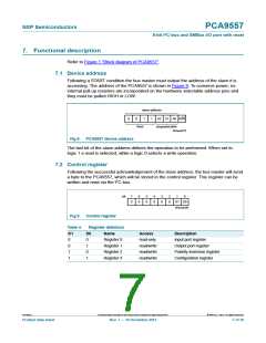
7.3 Register descriptions
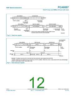
7.3.1 Register 0 - Input port register
This register is a read-only port. It reflects the incoming logic levels of the pins, regardless
of whether the pin is defined as an input or an output by the Configuration register. Writes
to this register have no effect.
Table 5.
Bit
Register 0 - Input port register bit allocation
7
6
5
4
3
2
1
0
Symbol
I7
I6
I5
I4
I3
I2
I1
I0
7.3.2 Register 1 - Output port register
This register reflects the outgoing logic levels of the pins defined as outputs by the
Configuration register. Bit values in this register have no effect on pins defined as inputs.
In turn, reads from this register reflect the value that is in the flip-flop controlling the output
selection, not the actual pin value.
Table 6.
Bit
Register 1 - Output port register bit allocation
7
O7
0
6
O6
0
5
O5
0
4
O4
0
3
O3
0
2
O2
0
1
O1
0
0
O0
0
Symbol
Default
7.3.3 Register 2 - Polarity inversion register
This register enables polarity inversion of pins defined as inputs by the Configuration
register. If a bit in this register is set (written with logic 1), the corresponding port pin’s
polarity is inverted. If a bit in this register is cleared (written with logic 0), the
corresponding port pin’s original polarity is retained.
Table 7.
Bit
Register 2 - Polarity inversion register bit allocation
7
N7
1
6
N6
1
5
N5
1
4
N4
1
3
N3
0
2
N2
0
1
N1
0
0
N0
0
Symbol
Default
7.3.4 Register 3 - Configuration register
This register configures the directions of the I/O pins. If a bit in this register is set, the
corresponding port pin is enabled as an input with high-impedance output driver. If a bit in
this register is cleared, the corresponding port pin is enabled as an output.
Table 8.
Bit
Register 3 - Configuration register bit allocation
7
C7
1
6
C6
1
5
C5
1
4
C4
1
3
C3
1
2
C2
1
1
C1
1
0
C0
1
Symbol
Default
PCA9557
All information provided in this document is subject to legal disclaimers.
© NXP B.V. 2013. All rights reserved.
Product data sheet
Rev. 7 — 10 December 2013
8 of 30

 NXP [ NXP ]