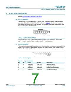
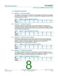
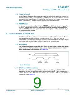
PCA9557
NXP Semiconductors
8-bit I2C-bus and SMBus I/O port with reset
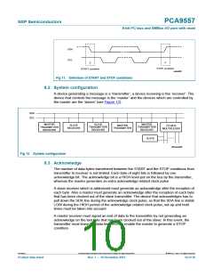
data output
by transmitter
not acknowledge
acknowledge
data output
by receiver
SCL from master
1
2
8
9
S
clock pulse for
START
condition
acknowledgement
002aaa987
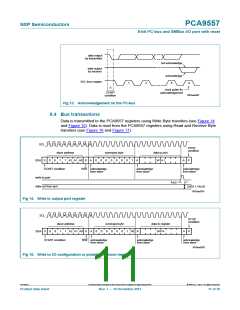
Fig 13. Acknowledgement on the I2C-bus
8.4 Bus transactions
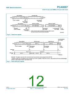
Data is transmitted to the PCA9557 registers using Write Byte transfers (see Figure 14
and Figure 15). Data is read from the PCA9557 registers using Read and Receive Byte
transfers (see Figure 16 and Figure 17).
SCL
1
2
3
4
5
6
7
8
9
STOP
condition
slave address
A2 A1 A0
command byte
data to port
DATA 1
SDA
S
0
0
1
1
0
A
0
0
0
0
0
0
0
1
A
A
P
START condition
R/W acknowledge
from slave
acknowledge
from slave
acknowledge
from slave
write to port
t
v(Q)
data out from port
DATA 1 VALID
002aad281
Fig 14. Write to output port register
SCL
1
2
3
4
5
6
7
8
9
STOP
condition
slave address
A2 A1 A0
command byte
data to register
DATA
SDA
S
0
0
1
1
0
A
0
0
0
0
0
0
1
1/0
A
A
P
START condition
R/W acknowledge
from slave
acknowledge
from slave
acknowledge
from slave
002aad282
Fig 15. Write to I/O configuration or polarity inversion registers
PCA9557
All information provided in this document is subject to legal disclaimers.
© NXP B.V. 2013. All rights reserved.
Product data sheet
Rev. 7 — 10 December 2013
11 of 30

 NXP [ NXP ]