PCA9557
NXP Semiconductors
8-bit I2C-bus and SMBus I/O port with reset
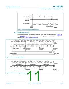
7. Functional description
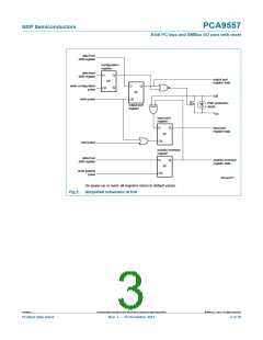
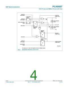
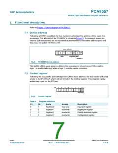
Refer to Figure 1 “Block diagram of PCA9557”.
7.1 Device address
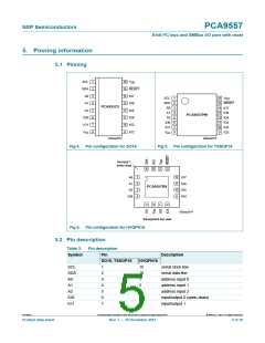
Following a START condition the bus master must output the address of the slave it is
accessing. The address of the PCA9557 is shown in Figure 8. To conserve power, no
internal pull-up resistors are incorporated on the hardware selectable address pins and
they must be pulled HIGH or LOW.
slave address
0
0
1
1
A2 A1 A0 R/W
fixed
programmable
002aad279
Fig 8. PCA9557 device address
The last bit of the slave address defines the operation to be performed. When set to
logic 1 a read is selected, while a logic 0 selects a write operation.
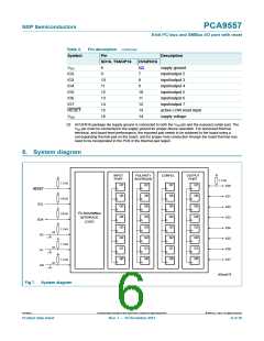
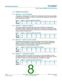
7.2 Control register
Following the successful acknowledgement of the slave address, the bus master will send
a byte to the PCA9557, which will be stored in the control register. This register can be
written and read via the I2C-bus.
bit:
7
0
6
0
5
0
4
0
3
0
2
0
1
0
D1 D0
002aad280
Fig 9. Control register
Table 4.
Register definition
D1
0
D0
0
Name
Access
Description
Register 0
Register 1
Register 2
Register 3
read-only
read/write
read/write
read/write
Input port register
Output port register
Polarity inversion register
Configuration register
0
1
1
0
1
1
PCA9557
All information provided in this document is subject to legal disclaimers.
© NXP B.V. 2013. All rights reserved.
Product data sheet
Rev. 7 — 10 December 2013
7 of 30

 NXP [ NXP ]