PCA9557
NXP Semiconductors
8-bit I2C-bus and SMBus I/O port with reset
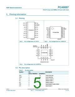
Table 3.
Pin description …continued
Symbol
Pin
Description
SO16, TSSOP16
HVQFN16
VSS
IO2
8
6[1]
supply ground
input/output 2
input/output 3
input/output 4
input/output 5
input/output 6
input/output 7
active LOW reset input
supply voltage
9
7
IO3
10
11
12
13
14
15
16
8
IO4
9
IO5
10
11
12
13
14
IO6
IO7
RESET
VDD
[1] HVQFN16 package die supply ground is connected to both the VSS pin and the exposed center pad. The
VSS pin must be connected to the supply ground for proper device operation. For enhanced thermal,
electrical, and board-level performance, the exposed pad needs to be soldered to the board using a
corresponding thermal pad on the board, and for proper heat conduction through the board thermal vias
need to be incorporated in the PCB in the thermal pad region.
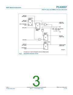
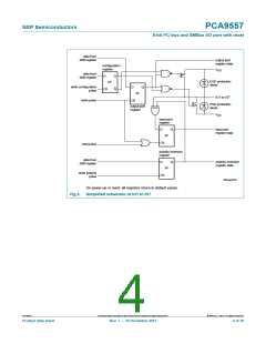
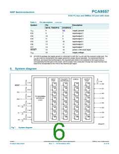
6. System diagram
INPUT
PORT
POLARITY
INVERSION
CONFIG.
Q7
OUTPUT
PORT
1.1 kΩ
1.1 kΩ
Q7
Q6
Q5
Q4
Q3
Q2
Q1
Q0
Q7
Q6
Q5
Q4
Q3
Q2
Q1
Q0
Q7
Q6
Q5
Q4
Q3
Q2
Q1
Q0
IO0
RESET
Q6
Q5
Q4
Q3
Q2
Q1
Q0
IO1
IO2
IO3
IO4
IO5
IO6
IO7
1.6 kΩ
SCL
2
I C-BUS/SMBus
1.6 kΩ
1.1 kΩ
1.1 kΩ
1.1 kΩ
INTERFACE
LOGIC
SDA
A2
or
or
or
A1
A0
002aad276
Fig 7. System diagram
PCA9557
All information provided in this document is subject to legal disclaimers.
© NXP B.V. 2013. All rights reserved.
Product data sheet
Rev. 7 — 10 December 2013
6 of 30

 NXP [ NXP ]