PCA9557
NXP Semiconductors
8-bit I2C-bus and SMBus I/O port with reset
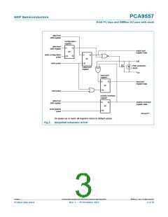
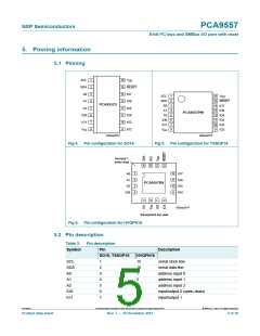
5. Pinning information
5.1 Pinning
1
16
15
14
13
12
11
10
9
SCL
SDA
A0
V
DD
2
3
4
5
6
7
8
RESET
IO7
1
2
3
4
5
6
7
8
16
15
14
13
SCL
SDA
A0
V
DD
RESET
IO7
A1
IO6
PCA9557D
A2
IO5
A1
IO6
PCA9557PW
12 IO5
IO0
IO1
IO4
A2
11
10
9
IO0
IO1
IO4
IO3
IO2
IO3
V
SS
IO2
V
SS
002aad272
002aad273
Fig 4. Pin configuration for SO16
Fig 5. Pin configuration for TSSOP16
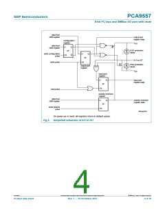
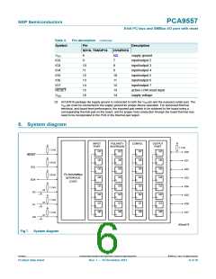
terminal 1
index area
1
2
3
4
12
11
10
9
A0
A1
IO7
IO6
IO5
IO4
PCA9557BS
A2
IO0
002aad274
Transparent top view
Fig 6. Pin configuration for HVQFN16
5.2 Pin description
Table 3.
Pin description
Symbol
Pin
Description
SO16, TSSOP16
HVQFN16
SCL
SDA
A0
1
2
3
4
5
6
7
15
16
1
serial clock line
serial data line
address input 0
address input 1
address input 2
input/output 0 (open-drain)
input/output 1
A1
2
A2
3
IO0
IO1
4
5
PCA9557
All information provided in this document is subject to legal disclaimers.
© NXP B.V. 2013. All rights reserved.
Product data sheet
Rev. 7 — 10 December 2013
5 of 30

 NXP [ NXP ]