Philips Semiconductors
Preliminary data
Low power, low price, low pin count (20 pin)
microcontroller with 4 kbyte OTP
87LPC764
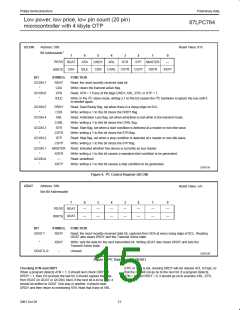
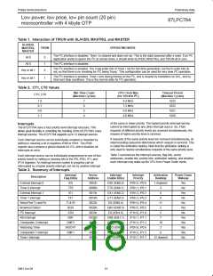
I2CFG
Address: C8h
Reset Value: 00h
Bit Addressable
7
6
5
4
3
2
1
0
SLAVEN MASTRQ CLRTI TIRUN
—
—
CT1
CT0
BIT
SYMBOL
FUNCTION
2
I2CFG.7
SLAVEN
Slave Enable. Writing a 1 this bit enables the slave functions of the I C subsystem. If SLAVEN and
2
2
MASTRQ are 0, the I C hardware is disabled. This bit is cleared to 0 by reset and by an I C
time-out.
2
I2CFG.6
MASTRQ
Master Request. Writing a 1 to this bit requests mastership of the I C bus. If a transmission is in
progress when this bit is changed from 0 to 1, action is delayed until a stop condition is detected. A
2
start condition is sent and DRDY is set (thus making ATN = 1 and generating an I C interrupt).
2
When a master wishes to release mastership status of the I C, it writes a 1 to XSTP in I2CON.
2
MASTRQ is cleared by an I C time-out.
I2CFG.5
I2CFG.4
CLRTI
TIRUN
Writing a 1 to this bit clears the Timer I overflow flag. This bit position always reads as a 0.
Writing a 1 to this bit lets Timer I run; a zero stops and clears it. Together with SLAVEN, MASTRQ,
and MASTER, this bit determines operational modes as shown in Table 1.
I2CFG.2, 3
—
Reserved for future use. Should not be set to 1 by user programs.
I2CFG.1, 0 CT1, CT0
These two bits are programmed as a function of the CPU clock rate, to optimize the MIN HI and LO
time of SCL when this device is a master on the I C. The time value determined by these bits
2
controls both of these parameters, and also the timing for stop and start conditions.
SU01474
2
Figure 8. I C Configuration Register (I2CFG)
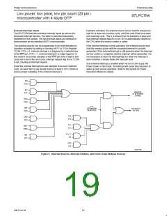
Regarding Software Response Time
first line of the table where CPU clock max is greater than or equal
to the actual frequency.
2
Because the 87LPC764 can run at 20 MHz, and because the I C
interface is optimized for high-speed operation, it is quite likely that
Table 2 also shows the machine cycle count for various settings of
CT1/CT0. This allows calculation of the actual minimum high and
low times for SCL as follows:
2
an I C service routine will sometimes respond to DRDY (which is set
at a rising edge of SCL) and write I2DAT before SCL has gone low
again. If XDAT were applied directly to SDA, this situation would
2
produce an I C protocol violation. The programmer need not worry
6 * Min Time Count
CPU clock (in MHz)
SCL min highńlow time (in microseconds) +
about this possibility because XDAT is applied to SDA only when
SCL is low.
2
Conversely, a program that includes an I C service routine may take
a long time to respond to DRDY. Typically, an I C routine operates
2
For instance, at an 8 MHz frequency, with CT1/CT0 set to 1 0, the
minimum SCL high and low times will be 5.25 µs.
on a flag-polling basis during a message, with interrupts from other
peripheral functions enabled. If an interrupt occurs, it will delay the
Table 2 also shows the Timer I timeout period (given in machine
cycles) for each CT1/CT0 combination. The timeout period varies
because of the way in which minimum SCL high and low times are
2
response of the I C service routine. The programmer need not worry
2
about this very much either, because the I C hardware stretches the
SCL low time until the service routine responds. The only constraint
on the response is that it must not exceed the Timer I time-out.
2
measured. When the I C interface is operating, Timer I is pre-loaded
at every SCL transition with a value dependent upon CT1/CT0. The
pre-load value is chosen such that a minimum SCL high or low time
has elapsed when Timer I reaches a count of 008 (the actual value
pre-loaded into Timer I is 8 minus the machine cycle count).
Values to be used in the CT1 and CT0 bits are shown in Table 2. To
2
allow the I C bus to run at the maximum rate for a particular
oscillator frequency, compare the actual oscillator rate to the f OSC
max column in the table. The value for CT1 and CT0 is found in the
14
2001 Oct 26

 NXP [ NXP ]