Philips Semiconductors
Preliminary data
Low power, low price, low pin count (20 pin)
microcontroller with 4 kbyte OTP
87LPC764
2
I C Serial Interface
2
The I C bus uses two wires (SDA and SCL) to transfer information
problems. SCL “stuck low” indicates a faulty master or slave. SCL
“stuck high” may mean a faulty device, or that noise induced onto
the I C bus caused all masters to withdraw from I C arbitration.
between devices connected to the bus. The main features of the
bus are:
2
2
• Bidirectional data transfer between masters and slaves.
2
The first five of these times are 4.7 ms (see I C specification) and
are covered by the low order three bits of timer I. Timer I is clocked
by the 87LPC764 CPU clock. Timer I can be pre-loaded with one of
four values to optimize timing for different oscillator frequencies. At
lower frequencies, software response time is increased and will
• Serial addressing of slaves (no added wiring).
• Acknowledgment after each transferred byte.
• Multimaster bus.
2
degrade maximum performance of the I C bus. See special function
• Arbitration between simultaneously transmitting masters without
register I2CFG description for prescale values (CT0, CT1).
corruption of serial data on bus.
The MAXIMUM SCL CHANGE time is important, but its exact span
is not critical. The complete 10 bits of timer I are used to count out
2
The I C subsystem includes hardware to simplify the software required
2
the maximum time. When I C operation is enabled, this counter is
2
to drive the I C bus. The hardware is a single bit interface which in
cleared by transitions on the SCL pin. The timer does not run
addition to including the necessary arbitration and framing error
checks, includes clock stretching and a bus timeout timer. The
interface is synchronized to software either through polled loops
or interrupts.
2
between I C frames (i.e., whenever reset or stop occurred more
recently than the last start). When this counter is running, it will carry
out after 1020 to 1023 machine cycles have elapsed since a change
2
on SCL. A carry out causes a hardware reset of the I C interface
Refer to the application note AN422, entitled “Using the 8XC751
and generates an interrupt if the Timer I interrupt is enabled. In
cases where the bus hang-up is due to a lack of software response
2
Microcontroller as an I C Bus Master” for additional discussion of
2
2
the 8xC76x I C interface and sample driver routines.
by this device, the reset releases SCL and allows I C operation
among other devices to continue.
2
The 87LPC764 I C implementation duplicates that of the 87C751
2
and 87C752 except for the following details:
Timer I is enabled to run, and will reset the I C interface upon
2
overflow, if the TIRUN bit in the I2CFG register is set. The Timer I
interrupt may be enabled via the ETI bit in IEN1, and its priority set
by the PTIH and PTI bits in the IP1H and IP1 registers respectively.
• The interrupt vector addresses for both the I C interrupt and the
Timer I interrupt.
2
• The I C SFR addresses (I2CON, I2CFG, I2DAT).
2
I C Interrupts
2
• The location of the I C interrupt enable bit and the name of the
2
2
If I C interrupts are enabled (EA and EI2 are both set to 1), an I C
interrupt will occur whenever the ATN flag is set by a start, stop,
arbitration loss, or data ready condition (refer to the description of ATN
following). In practice, it is not efficient to operate the I C interface in
this fashion because the I C interrupt service routine would somehow
have to distinguish between hundreds of possible conditions. Also,
since I C can operate at a fairly high rate, the software may execute
faster if the code simply waits for the I C interface.
SFR it is located within (EI2 is Bit 0 in IEN1).
• The location of the Timer I interrupt enable bit and the name of the
2
SFR it is located within (ETI is Bit 7 in IEN1).
2
2
• The I C and Timer I interrupts have a settable priority.
2
2
Timer I is used to both control the timing of the I C bus and also to
2
detect a “bus locked” condition, by causing an interrupt when
2
2
Typically, the I C interrupt should only be used to indicate a start
nothing happens on the I C bus for an inordinately long period of
condition at an idle slave device, or a stop condition at an idle master
time while a transmission is in progress. If this interrupt occurs, the
program has the opportunity to attempt to correct the fault and
resume I C operation.
2
device (if it is waiting to use the I C bus). This is accomplished by
2
2
enabling the I C interrupt only during the aforementioned conditions.
2
Six time spans are important in I C operation and are insured by timer I:
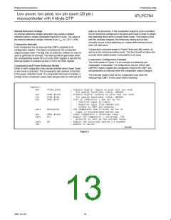
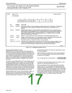
Reading I2CON
RDAT
The data from SDA is captured into “Receive DATa”
whenever a rising edge occurs on SCL. RDAT is also
available (with seven low-order zeros) in the I2DAT
register. The difference between reading it here and
there is that reading I2DAT clears DRDY, allowing the
• The MINIMUM HIGH time for SCL when this device is the master.
• The MINIMUM LOW time for SCL when this device is a master.
This is not very important for a single-bit hardware interface like
this one, because the SCL low time is stretched until the software
2
2
responds to the I C flags. The software response time normally
I C to proceed on to another bit. Typically, the first
meets or exceeds the MIN LO time. In cases where the software
responds within MIN HI + MIN LO) time, timer I will ensure that
the minimum time is met.
seven bits of a received byte are read from
I2DAT, while the 8th is read here. Then I2DAT can be
written to send the Acknowledge bit and clear DRDY.
• The MINIMUM SCL HIGH TO SDA HIGH time in a stop condition.
ATN
“ATteNtion” is 1 when one or more of DRDY, ARL, STR, or
STP is 1. Thus, ATN comprises a single bit that can be
tested to release the I C service routine from a “wait loop.”
2
• The MINIMUM SDA HIGH TO SDA LOW time between I C stop
2
2
and start conditions (4.7ms, see I C specification).
DRDY
“Data ReaDY” (and thus ATN) is set when a rising edge
occurs on SCL, except at idle slave. DRDY is cleared
by writing CDR = 1, or by writing or reading the I2DAT
register. The following low period on SCL is stretched
until the program responds by clearing DRDY.
• The MINIMUM SDA LOW TO SCL LOW time in a start condition.
2
• The MAXIMUM SCL CHANGE time while an I C frame is in
progress. A frame is in progress between a start condition and the
following stop condition. This time span serves to detect a lack of
2
software response on this device as well as external I C
11
2001 Oct 26

 NXP [ NXP ]